
Copyright © 2010-2011,
Thomas Schmid,
Ye-Sheng Kuo,
Matt Smith,
Lohit Yerva,
and Prabal Dutta.
See posted lab schedule for due dates, in-lab, and post-lab due dates.
The purpose of this lab is to understand the concept of interrupts in embedded systems.

Interrupts are similar to branch instructions in regular code - they are both used to redirect code flow in a program. Branches occur naturally and somewhat predictably in code. Interrupts are usually generated by external physical sources and are generally unpredicable. The most basic interrupt model would involve taking the 370 LC2K pipeline and adding a button input that, when pressed, makes the processor jump to "Button_Pressed" Interrupt Request (IRQ) Handler (basically a fancy function), which increments button pressed count. A basic Interrupt Controller (IC) would accept the button input, store the current PC register address in a "Link Register", and load the PC register with address of the "Button_Pressed" function (always in the same location) in the next cycle. When the interrupt is done, the IC can load the previous PC register address from the "Link Register" back into the PC register so that the main program can continue executing as before the interrupt. This is the fundemental idea behind the interrupts - random external events can be used to signal the processor to stop what it's doing, and do something else that is more important right now.
Interrupts are a fundamental mechanism in embedded systems to let the microcontroller know about events. On the Cortex-M3 core, the Nested Vectored Interrupt Controller (NVIC) allows the core to configure interrupt handling. Interrupts are also a key to low-power designs, where the core is in deep-sleep mode and only wakes up if it needs to handle an interrupt.
In Lab 3, you learned how to write a peripheral in the FPGA fabric and how to interface it over the APB3 bus to the microcontroller. So far, the only access you had to your peripheral was through memory mapped I/O, i.e., you either read or wrote a register to get data from or to the peripheral, respectively. For example, you had to specifically poll the switch status in order to see if it is pushed or released. This is not ideal as the core has to busy-loop and poll the I/O line continuously, wasting precious resources. It would be better if the microcontroller could go about its business but still get interrupted when a person pushes a button.
Q: In Lab 3, you had two modules attached to the APB3 bus. What is the difference in bytes between the memory mapped addresses of the two modules? (Hint: Use the Modify Memory Map function in Libero)
First, download the Lab 4 FPGA project.
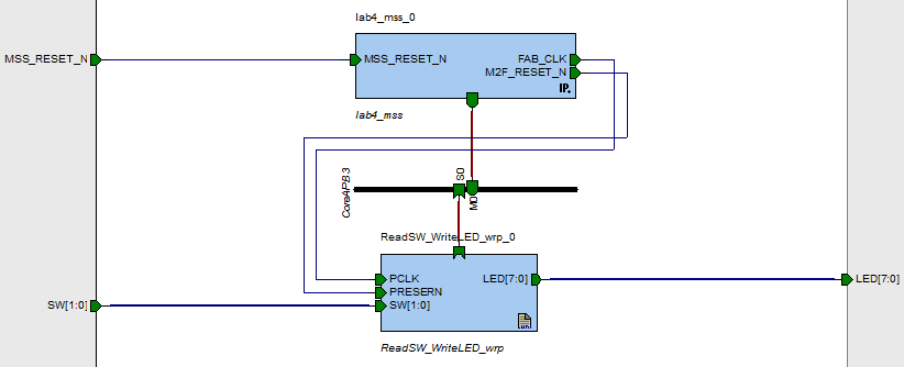
This hardware is similar to the final Lab 3 hardware, but notice that we have combined the switches
read register and LEDs write register into one peripheral.
Our single FPGA peripheral module (ReadSW_WriteLED_wrp) has two inputs, SW[1:0]
and eight outputs, LED[7:0]. If you got the above answer right, you knew that each peripheral
on the APB3 bus is allocated 256 bytes of address. Therefore, inside the peripheral we can address
more than one 32bit (4 byte) register(s). The peripheral has two memory locations: 0x40050000
for read/write of a 3 bit LED register and 0x40050004 for the read of
2 bits of switches. Writing to location 0x40050004 is ignored.
The value of the 3 bit LED register indicates which one of the 8 LEDs to turn on. Internally, the leds are driven by a 3 bit to 8 bit decoder module to control the individual LED signals.
Q: Look inside ReadSW_WriteLED.v. What input wires/variable determines which register (led or sw) are accessed? What is connected to subAddr in the wrapper? Why do we only use the lower 8 bits of the PADDR?
Be sure that the two SW[1:0] inputs are connected to the two switches SW1 and SW2, and the LED[7:0] are connected to the 8 LEDs. Then program your evaluation kit with the code.
The Soft Console application consists of a counter that gets incremented or decremented by pushing one of the switches. Upon a change, the counter value is written into the memory location of our peripheral LED output.
Create a new minimum running assembly project using the 373 SoftConsole Assembly Readme. Create a new main.s file with the following content:
Button Polling Code
	.text
	.syntax	unified
	.thumb

	.global main
	.type	main, %function
main:
	@ Load LEDs memory map address into r0
	mov	r0, #0
	movt	r0, #:upper16:0x40050000
	@ Load Switches memory map address into r1
	movw	r1, #:lower16:0x40050004
	movt	r1, #:upper16:0x40050004

	mov	r2, #0	@ int counter = 0
	mov	r3, #0	@ int switches = 0
	mov	r4, #0	@ tmpSw = 0

	mov	r5, #0
	str	r5, [r0, #0]	@ LEDs = 0
	ldr	r3, [r1, #0]	@ Read mem map Switches into switches
	mvn	r3, r3		@ Active low switches

while1:
	ldr	r4, [r1, #0]	@ Read mem map Switches into tmpSw
	mvn	r4, r4		@ Active low switches

	@ if(switches == tmpSw) then goto loop
	sub	r5, r4, r3
	cbnz	r5, check_SW1
	b	while1

	@ else - something changed in the switches
check_SW1:
	ands	r5, r5, #1	@ switches & 0x1
	cbz	r5, check_SW2	@ if( switches & 0x1 == 0 ) goto check_SW2
	ands	r6, r4, #1	@ tmpSw & 0x1
	cbnz	r6, check_SW2	@ if( tmpSw & 0x1 == 1 ) goto check_SW2
	sub	r2, #1		@ counter--

check_SW2:
	ands	r5, r3, #2		@ switches & 0x2
	cbz	r5, saveSWs_setLEDs	@ if( switches & 0x2 == 0) goto saveSWs_setLEDs
	ands	r6, r4, #2		@ tmpSw & 0x2
	cbnz	r6, saveSWs_setLEDs	@ if( tmpSw & 0x2 == 1) goto saveSWs_setLEDs
	add	r2, #1			@ counter++

saveSWs_setLEDs:
	mov	r3, r4		@ switches = tmpSw
	str	r2, [r0, #0]	@ LEDs = counter

	b	while1
	.size	main, .-main
Program your board with your application in the SRAM. Start the debugger and resume your application. Try pushing the switches SW1 and SW2. The LED should go up or down respectively. However, notice that sometimes, the LED jumps several LEDs at once. This is a common artifact of switches that are not properly debounced. The problem is that the switch itself does not provide a clean high-low transition, but flips back and forth several times. Our application runs fast enough to catch this.
Connect the oscilloscope to the switch, and try to look at the cases where the LED jumps several positions, even though you pressed only once. Keep a screenshot of one of the captures for postlab.
There are two major problems with this application:
There are several ways the FPGA can interrupt the Cortex-M3. The most common way will be through the Fabric Interrupt (FABINT). This is a dedicated interrupt line just for the fabric. Another way we will explore later is through the I/O lines of the Cortex-M3. We will use this method later, when we want more than one interrupt. The main difference between FABINT and interrupting through I/O lines is that FABINT is a level triggered interrupt, while the I/O lines can be configured for positive, negative, or both edge triggering.
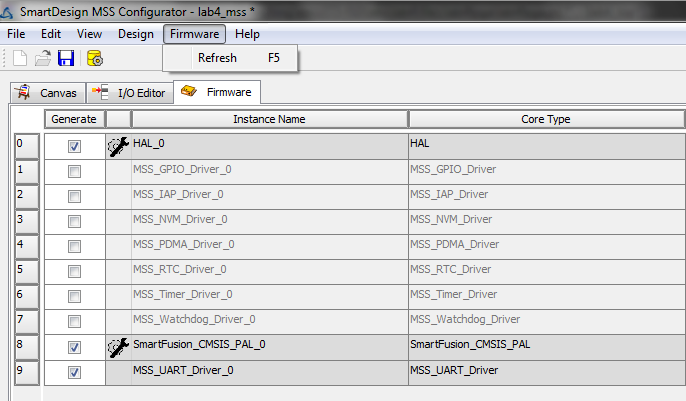
Open up the Smart Design MSS Configurator. First of all, add a checkmark to the UART_0 component. This doesn't have anything to do with interrupts. But we will use the UART_0 to plot some interesting information.
Once you added the checkmark to the UART_0 component, click on the
Firmware tab. Then click the menu Firmware > Refresh or hit
F5. The MSS_UART_Driver_0 should have appeared now. Make sure it has a
checkmark in front of it. We will use this later in our code to talk to the
UART component. If MSS_UART_Driver_0 does not appear after refresh, then save, close and reopen
the MSS Configurator. If it requests you to download the core firmeware, then do it. You can ignore the
download symbol ![]() in front of the other core firmwares.
in front of the other core firmwares.
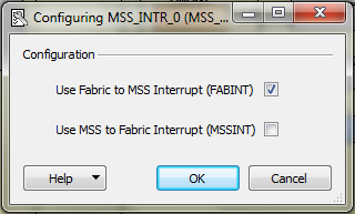
Now, go back to the canvas view and click on the Interrupt Management block on the lower left-hand corner of the configurator. Make a checkmark next to the FABINT line. This will enable the fabric interrupt and allow you to connect to it in the smart designer.
Generate the configuration by clicking  and return back
to Libero. We will now add the FABINT capabilities to the existing Verilog
code.
and return back
to Libero. We will now add the FABINT capabilities to the existing Verilog
code.
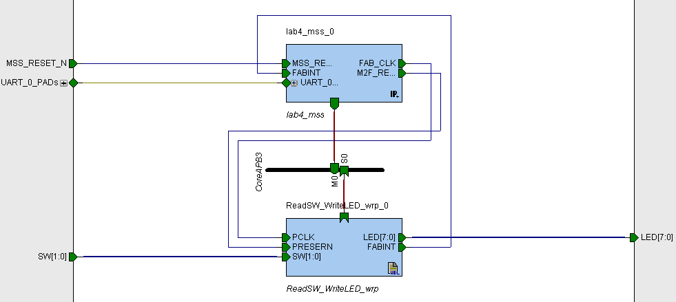
First, we have to update our SmartDesign. In Libero, click on the lab4_top component. You will notice that Libero already loaded your newly generated MSS code. But it did not update its visual representation. Right click on the lab4_mss_0 IP component and select Update Instance(s) with Latest Component. You will notice that the UART connection was added automatically and promoted to the top level. In addition, we got a FABINT port.
Next, double-click on the ReadSW_WriteLED_wrp. This will open the Verilog code. Add another output called FABINT to this component. Then, bring FABINT into the ReadSW_WriteLED module.
First, delete the always@* block inside the ReadSW_WriteLED module. We have to replace this block
with logic that generates an interrupt when either one of the push buttons
gets pressed. To do so, we will have to
clksw_reg register to indicate which switch we
pressedSynchronization of the asynchronous switch is necessary to avoid glitches. We can perform this with the following block:
/* Synchonization of Asynchronous switch input */
always@(posedge clk)
begin
	sw0_pulse[0] <= ~sw_port[0];
	sw0_pulse[1] <= sw0_pulse[0];
	sw0_pulse[2] <= sw0_pulse[1];
end
Add the necessary register(s) to your module, and a second block similar to this one for
sw_port[1]. Remember only a register variable can be assigned in the always block.
Q: Explain in a few sentences how this block synchronizes the input switch.
Q: Why is the switch input inverted?
Q: What happens if the sw_port[0] pulse is shorter than one PCLK period?
This is a more robust synronization block that solves the above problem. Answer the following questions on this code.
Q: How does this code solve the shorter than one PCLK period sw_port[x] pulse problem?
Now, we have to generate the interrupt pulse. Unfortunately, we can not directly use the output of the switch synchronizer because the FABINT is a level-triggered interrupt. Therefore, we have to generate a pulse, instead of just a rising edge. Fortunately, our synchronizer generates all the signals to do so. The following code will generate a pulse every time either one of the switches gets pressed.
 /* Pulse detection and pulse generation logic */

assign sw0_int = (sw0_pulse[1] == 1'b1) & (sw0_pulse[2] == 1'b0);
assign sw1_int = (sw1_pulse[1] == 1'b1) & (sw1_pulse[2] == 1'b0);

always@(posedge clk)
if(~nreset)
	begin
	FABINT <= 1'b0;
	end
else
	begin
	if(sw0_int)
		begin
		FABINT <= 1'b1;
		end
	else if(sw1_int)
		begin
		FABINT <= 1'b1;
		end
	else
		begin
		FABINT <= 1'b0;
		end
	end
sw_reg
So far, we interrupted the Cortex-M3, but we have no way to find out which
switch got pressed. Extend the code such that the sw_reg
indicates which switch got pressed, i.e., if bit 0 is set, then switch 0 got
pressed, and if bit 1 is set, then switch 1 got pressed. The
sw_reg register should get reset to 0 upon reading it ( and only it) from the
Cortex-M3. This is a common behavior for peripheral interrupt status registers.
Remember assign statements only work with wires.
You will have to check and update your ReadSW_WriteLED_wrp component and regenerate the smart design before you can synthesize your project. For this, go back to the smart design lab4_top, right click on ReadSW_WriteLED_wrp and update the component. If the Update Instance(s) with Latest Component is not available, then use Check HDL to remove all errors from the updated files.
Make the necessary connections by selecting both ends of the wire while holding shift and then right-click a port. Select the Connect option. Your block diagram should now look like this.
Generate your Smart Design, and then synthesize, place and route, and program your evaluation board with the code. It is now time to update your source code.
As mentioned earlier, we will use the UART_0 for some additional debugging information. For that purpose, modifiy the current assembly project to add interrupts and printf373 by reading through the 373 SoftConsole Assembly Readme section "Create fully capable assembly code (Interrupts and printf373)" that follows the "Create minimum running assembly code". Keep the current main.s file. Exclude startup.s from the build process (Right-Click on the filename -> Exclude from build.... Read the How to use printf373() with assembly section of readme.
You will learn more about serial interfacing in Lab 5.
First, add a printf373 call to print your name right at the
begining of main. This will indicate that your application has started.
To receive the characters on your computer, start HyperTerminal or PuTTY and set the session to 57600 baud, 8 bits data, 1 stop bit, no parity, and no flow control. Follow the HyperTerminal or Putty setup in the 373 SoftConsole Assembly Readme.
Go ahead and launch your HyperTerminal or PuTTY session now. Once we start our application, you will see some text appear on it.
Next, we will have to declare our interrupt handling service routine.
Fortunately, the Actel SoftConsole already provisioned the interrupt vector
with some weak links. Open the file startupWithInt.s. The first global definition you
see, intVectors is the so called interrupt vector. It defines
the link between interrupt number, and function to jump to if this interrupt
happened. In our case, all the function names are already defined. However,
the functions themselves only exist as weak links, i.e., you can
overwrite them with your own functions. Look at Chapter 1: ARM Cortex-M3 Microcontroller -> Interrupts
of
Actel SmartFusion Microcontroller Subsystem User's Guide from prelab.
Scroll down until you find the name of the FABINT Interrupt Service Routine (ISR). Then
scroll even further down until you find the weak link for this function. Next,
create a new file called interrupts.s and create a new function with that exact name.
Add the following to top of the file.
waitStr: 	.asciz "Handling IRQ FABINT %d\n\r"
	.align 2

@ Global variables (must be in the .data section)
	.data
count:	.word	0

	.text
	.syntax	unified
	.thumb
Inside the Fabric Interrupt Service Routine (ISR), add a printf373 statement that outputs the number
of times this function was called so far using the waitStr defined above. This will help you visualize the
UART output and understand how often the interrupt fired. Remember that an ISR automatically saves r0-r3, lr, and sp.
However, it does not save r4-r12. Keep this in mind when modifying the Fabric ISR code.
There are two more things we have to do before the NVIC will treat our interrupts correctly.
main
functionIf we don't perform point 1., then our interrupt service routine will never get handled. If we don't perform point 2., then the interrupt will fire again as soon as you left your interrupt service routine, because the interrupt routine code never told the hardware that it accepted the interrupt request.
Read Chapter 6: Nested Vectored Interrupt Controller of Cortex-M3 Technical Reference Manual. Notice the eight Interrupt Set-Enable and Clear-Pending registers address under 6.3: NVIC programmers model. Read Chapter 1: ARM Cortex-M3 Microcontroller -> Interrupts of Actel SmartFusion Microcontroller Subsystem User's Guide. Notice the Nested Interrupt Vector Controller (NVIC) table. It lists the IRQ number x (INTISR[x]) for all the interrupt names defined in the startupWithInt.s assembly file that you added to your project.
In the interrupts.s file that includes the Fabric ISR add the following functions. Write the following assembly function based on lecture notes and reference guides.
Please write the void EnableIRQ(int irq_num) function using the following template:
@ Enable the IRQ
@ Inputs: IRQ number in r0
@ Output:
	.global	EnableIRQ
	.type	EnableIRQ, %function
EnableIRQ:
	push	{r4,r5} @ Callee Save

	@ Load NVIC_ISER (Set-Enable Registers) start address

	@ Select register to modify

	@ Select bit to set in the register

	@ Set bit

	pop	{r4,r5}
	bx	lr
Please write the void ClearPendingIRQ(int irq_num) function using the following template:
@ Clear the pending the IRQ
@ Inputs: IRQ number in r0
@ Output:
	.global	ClearPendingIRQ
	.type	ClearPendingIRQ, %function
ClearPendingIRQ:
	push	{r4,r5} @ Callee Save

	@ Load NVIC_ICPR (Clear-Pending Registers) start address

	@ Select register to modify

	@ Select bit to set in the register

	@ Set bit

	pop	{r4,r5}
	bx 	lr
Now clear pending and enable the Fabric interrupt in the main function, and clear pending inside the Fabric interrupt handler function. You need to save (push and pop) one register inside the Fabric interrupt handler to handle function calls correctly. Figure out which one.
Make sure that you are not overwriting registers (arguments) when you call these functions in existing code.
Connect the terminal to the serial port and program your board with your application. Then, start the debugger and launch your application. Observe the output of the terminal. You should first see your name. Then, press the switches. You should see a new line for every time you press the switches.
Q: Pause  your debugging session and add a breakpoint
to one of the interrupt service routines. Resume
your debugging session and add a breakpoint
to one of the interrupt service routines. Resume  the operation and hit one of the switches. Your debugger should stop right at
your breakpoint. Inspect the disassembled code. Which registers are used by
the interrupt routine?
the operation and hit one of the switches. Your debugger should stop right at
your breakpoint. Inspect the disassembled code. Which registers are used by
the interrupt routine?
It is now time to change the application behavior. Until now, the LED's are
still controlled by polling the sw_reg register. This introduces
a significant latency. Change the application such that the reading of
sw_reg is done inside the interrupt service routine. Then and replace
the code inside the while1 loop with the following code and add
the "waitStr" to your code:
while1:
	movw	r0,	#:lower16:waitStr	@ "Wait For Interrupt\n\r"
	movt	r0,	#:upper16:waitStr
	bl	printf373
	wfi		@Wait For Interrupt; Stop execution until an interrupt fires
	b	while1
The Wait for Interrupt instruction tells the processor to stop executing any more instructions until an interrupt fires. This idles the processor and saves power.
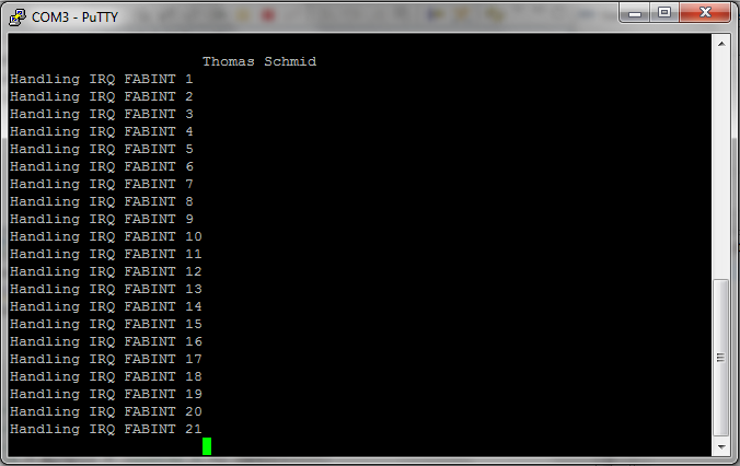
Program your new application on your board and start it. Your output on the terminal should look similar to the picture below.
After the Wait For Interrupt,wfi, instruction is the SoftConsole debugger might disconnect from the board. Basically, you will get a debugger error. You will not be able to stop and reprogram it. You just need to disconnect and reconnect the board, if this happens.
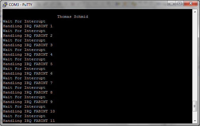
Q: Explain in two sentences why we have the text Wait For Interrupt in between every interrupt service routine.
Replace your while loop in your main function
with an empty busy loop:
while1:
	b while1
Until now, we only had to deal with one interrupt source. However, what happens if we have several potential interrupt sources? Especially in the case where they fire concurrently, which one will be treated first? Fortunately, the NVIC has many possibilities to configure its behavior. But first, we have to reconfigure our hardware.
The FABINT is only one way to interrupt the Cortex-M3. Another interrupt source are the I/O lines. They can be configured to fire an interrupt on a specific edge (falling or rising), or on both edges. And since we can connect the I/O lines to the fabric, we can use them to provide multiple interrupt lines from the FPGA to the Cortex-M3.
Open up the MSS Configurator and double-click on the GPIO module. Add one I/O line as input, and one line as output.
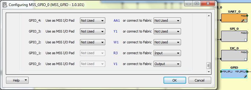
Next, click on the Firmware tab and make sure that there is a check mark next
to the MSS_GPIO_Driver_0. Then generate your design by clicking .
Edit the ReadSW_WriteLED_wrp component and add 2 additional outputs. Assign the value of FABINT to both the outputs. This will assure that all three interrupts get generated at the same time.
Go back to the canvas of your Smart Designer block diagram and update both components. Connect the second FABINT interrupt output to the GPIO input of the MSS, promote the third FABINT interrupt output to the top, and promote the GPIO output to the top. Your connections should look similar to the following:
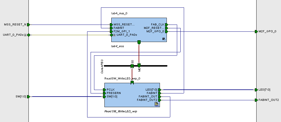
Next, go to the I/O Attribute Editor and connect M2F_GPO_0 output to USER I/O pin 1 (J19), and connect FABINT_OUT2 to USER I/O pin 2 (J20). Then, GENERATE your Smart Design, synthesize, place and route, and program your FPGA with it.
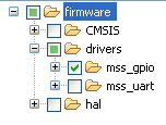
Once you programmed the FPGA, open up SoftConsole to edit your application. First, we add the GPIO drivers created by the MSS Configurator. Perform the same steps as you did for the UART drivers. However, this time select the mss_gpio directory instead of the mss_uart directory.
Make sure that you are not overwriting registers (arguments) when you call these functions in existing code.
In our main function, we have to initialize the GPIO
driver. Add the following commands. All the MSS_GPIO_x functions are defined
in drivers/mss_gpio/mss_gpio.h.
bl MSS_GPIO_init @no argumentsNext, we have to configure the GPIO pins. Note that this is similar to what you performed in your gpio library written in Lab 2. First, we configure the output GPIO:
@ Config GPIO 0 as output
mov	r0, #0	@ MSS_GPIO_0
mov	r1, #0x000000005	@ MSS_GPIO_OUTPUT_MODE
bl	MSS_GPIO_config
Then, we configure the input as an interrupt. The interrupt should fire on a rising edge.
@ Config GPIO 1 as input with interrupts
mov	r0, #1	@ MSS_GPIO_1
mov	r1, #0x000000042	@ MSS_GPIO_INPUT_MODE | MSS_GPIO_IRQ_EDGE_POSITIVE
bl	MSS_GPIO_config
bl	MSS_GPIO_enable_irq	@ 1 argument, MSS_GPIO_1

mov	r0, #32	@ GPIO0_IRQHandler
bl	EnableIRQ
Now all we have left is to add the interrupt service routine for GPIO1 input to interrupt.s:
	.global	GPIO1_IRQHandler
	.type	GPIO1_IRQHandler, %function
GPIO1_IRQHandler:
	@ Pulse GPIO0 output
	mov	r0, #0		@ MSS_GPIO_0
	mov	r1, #0x1	@ set GPIO0 output high
	bl	MSS_GPIO_set_output

	@ Print interrupt string
	movw	r0, #:lower16:GPIO1intStr @ "Interrupt occurred - GPIO 1 \n"
	movt	r0, #:upper16:GPIO1intStr
	bl	printf373

	@ Clear MSS GPIO pending
	mov	r0, #1
	bl	MSS_GPIO_clear_irq

	mov	r0, #0		@ MSS_GPIO_0
	mov	r1, #0x0 	@ set GPIO0 output low
	bl	MSS_GPIO_set_output

	bx	lr
Q: Explain in a few sentences what the MSS_GPIO_* functions exactly do. Especially, which registers do they modify? What other functions are provided by the MSS_GPIO drivers? List all of them with one sentence per function explaining its purpose.
Before you run the application, note on a paper your guess of which interrupt, GPIO1 or FABINT fires first. Don't show it to your lab partner yet!
Q: Run the application you just wrote on your board and connect a serial terminal to the serial port. Push the switch several times. Which of the two interrupts fires first? Compare it to your answer that you just wrote down. Explain in two sentences why this interrupt gets handled before the other one.
As you can imagine, it takes time from the interrupt generation in the fabric, until the Cortex-M3 actually processes the interrupt in software. This is usually called "Interrupt Latency". We will next investigate this latency to better understand its characteristics.
Use the oscilloscope and connect a probe to each of the User I/O lines created above (M2F_GPO_0 and FABINT_OUT2). Configure the trigger to be sourced from the FABINT_OUT2 line, and use the "Normal" or "One Shot" mode. Then, press a switch and measure the time between fab interrupt and toggling of the I/O line from the MSS.
Be aware that printf takes a fair bit of time to go over the serial line. Do not let the printf373 happen before you toggle the I/O line.
Q: Perform 10 latency measurements. What is the mean time and standard deviation of your measurements?
Your measurements should be fairly consistent, without too much jitter. This is because the Cortex-M3 is not very busy. Especially, in our current application, we do not have any blocks that disable interrupts.
Sometimes, an embedded system has to execute a code sequence that should not be interrupted. For example, if we modify a global variable that could also be modified in an interrupt routine, then we should disable interrupts before we start modifying, and re-enable them once done. This avoids concurrency issues. To turn off all interrupts, except hard faults, on the Cortex-M3, you can use the following assembler command:
cpsid iTo re-enable them, use the following command
cpsie iThis code modifies the PRIMASK.
Let's measure the interrupt latency again, but this time we add a non interruptable for loop into the main while loop. Modify the infinite while loop to
while1:
	cpsid	i
	mov	r0,	#0
loop:
	cmp	r0,	#100
	add	r0, r0, #1
	bne.n	loop
	cpsie	i
	b	while1
and measure the interrupt latency.
Q: Perform 10 latency measurements with PRIMASK. What is the mean time and standard deviation of your measurements? Explain the behavior in two sentences.
In class you learned about the Nested Vectored Interrupt Controller (NVIC) and how it can handle priorities and groups for different interrupt sources. We will now use the NVIC to change the interrupt priority such that the interrupt that came first, now becomes second.
Write the following assembly function based on lecture notes and reference guides. Use the above EnableIRQ as an example.
Read Chapter 6: Nested Vectored Interrupt Controller of Cortex-M3 Technical Reference Manual. Every byte or 8bits of a NVIC_IPR0-59 registers determines what priority group each interrupt fall into. For example, irq0-irq3 (INTISR[0]-INTISR[3]) fall into the 4byte (32bit) NVIC_IPR0 register's byte0-byte3. Higher priority groups can interrupt the lower ones. Smartfusion has 32 priority levels. Therfore, only the top 5bits of the byte are implemented.
void SetIRQPriority (int IRQn, char PriorityGroup)
IRQn is the interrupt number and char is int8
Modify your code using the above function such that the interrupt that was first, now becomes second. Execute your application and verify that it works using the terminal.
Make sure that you are not overwriting registers (arguments) when you call these functions in existing code.
Changing the priority of an interrupt changes the order at which interrupts get handled. But what happens if an interrupt fires while another interrupt is still getting processed? Interrupt service routines are not protected from other interrupts if they have a higher priority (lower priority number). To illustrate this, let's add a delay between the two interrupts that so far fired at the same time, such that one of the interrupts comes later than the other.
The following code is a delay loop using a counter to the ReadSW_WriteLED module. Add it to your Verilog
module code and adapt it such that the second interrupt (named
FABINT_OUT in my code) fires later than the FABINT
interrupt.
reg [31:0]  counter;
reg counter_en;
reg fabintOut;

assign FABINT_OUT = fabintOut;

always@(posedge clk)
begin
if(~nreset)
    begin
    counter <= 32'h00000000;
    fabintOut   <= 1'b0;
    counter_en <= 1'b0;
    end
else if(FABINT)
    begin
    counter <= 32'h00000000;
    counter_en <= 1'b1;
    fabintOut <= 1'b0;
    end
else if(counter_en)
    begin
    if(counter == 32'h00004FFF)
        begin
        counter <= counter + 1;
        counter_en <= 1'b0;
        fabintOut <= 1'b1;
        end
    else if(counter == 32'h00005000)
        begin
        counter <= 32'h00000000;
        counter_en <= 1'b0;
        fabintOut <= 1'b0;
        end
    else
        begin
        counter <= counter + 1;
        counter_en <= 1'b1;
        fabintOut <= 1'b0;
        end
    end
else
    begin
    counter <= 32'h00000000;
    counter_en <= 1'b0;
    fabintOut <= 1'b0;
    end
end
Program your SmartFusion with this addition, and look at the output of the
terminal. Make sure that the later interrupt has a higher priority (lower
priority number) in your SoftConsole code. Your output should look similar to
the following picture. If it doesn't then most likely some of your clock
subsystem is differently configured. If this is the case, ask a lab assistant
for help.
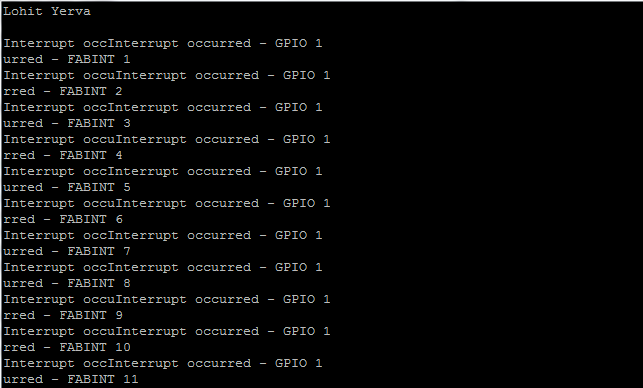
Q: Explain the output behavior in 2 sentences. The character shifts are due to slight time drift in the system.
Q: Explain at least two methods on how to avoid this problem. Hint: PRIMASK
Part 1: Write a debouncer for the switches, either in assembly (hint: clear interrupt flags) or in verilog (hint: counters). The concept of the debouncer is simple: after the first switch event detected, ignore any subsequent events from that switch for a short period of time.
Part 2: Write a single memory mapped verilog component device that generates an interrupt every X clock ticks. Make this component into a peripheral such that the Cortex-M3 can start, stop, reset, and change X by writing to its registers. Multiple registers should be accessed in one module like the ReadSW_WriteLED module given. Write a small application using your peripheral and toggle an LED whenever your peripheral generates an interrupt.