Due to the unique advantages of the hemispherical image sensor such as a wide field of view and low aberrations with less optical and mechanical components in the system, various strategies have been proposed to implement optoelectronic devices on non-planar surfaces. And they are crucial to realize imaging systems on hemispherical surface.
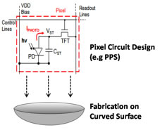
In this project, we demonstrated the feasibility of using maskless laser write lithography (LWL) with level-to-level alignment capability to realize a high performance amorphous silicon thin-film transistor (a-Si:H TFT) passive pixel sensor (PPS) on flat and curved surfaces.
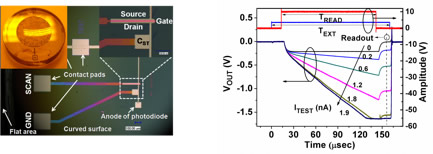
The obtained experimental results show that it is possible to realize 128x128 a-Si:H TFT active-matrix PPS with a pixel pitch of 50 to 150 µm and a dynamic range of about 40 dB. Figure below shows some of the experimental results; (left) photograph of the fabricated substrate PPS circuit (right) oscilloscope traces of VOUT for different ITEST. Further integration of the proven solution-processable organic photodetectors will allow realizing a high resolution hemispherical image sensor. This work was done in collaboration with the Fraunhofer Institute for Applied Optics (Jena, Germany) and is supported by DARPA/MTO HARDI Program.
G. Yoo et al., Sensor and Actuator A: Physical, 158 (2010) 280.

 Due to the unique advantages of the hemispherical image sensor such as a wide field of view and low aberrations with less optical and mechanical components in the system, various strategies have been proposed to implement optoelectronic devices on non-planar surfaces. And they are crucial to realize imaging systems on hemispherical surface.