Electrical Properties of Dual-Gate Amorphous Indium-Gallium-Zinc-Oxide(a-IGZO) TFTs
Gwanghyeon Baek, Alex Kuo and Jerzy Kanicki
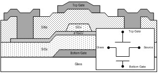
Structure of Dual-Gate a-IGZO-TFT
Amorphous In-Ga-Zn-O (a-IGZO) thin-film transistor (TFT) has shown promised for high quality display and imaging applications. To enhance its electrical and optical characteristics, dual-gate structure is introduced.
After forming bottom gate on glass wafer using molybdenum (Mo), a PECVD was used to deposit the silicon oxide gate insulator (200 nm), and the a-IGZO film was sputtered. After the island a-IGZO definition, a 150 nm sputtered followed by a deposition of 300 nm of passivation silicon nitride layer. Next, the source / drain contact vias were formed, followed by the sputtering and patterning of source/drain electrode and top gate.
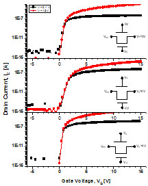
The measured transfer characteristics show that both top and bottom gate can control channel region. Since dielectric layer between top gate and channel region has lower gate capacitance than the one over bottom gate, the TFT has larger sub-threshold swing (S) and lower on current (Ion). By applying same bias both on bottom and top gates simultaneously, small S and higher Ion are achieved in comparison to biasing either top or bottom gate. Top gate metal also would work as the light shield to protect channel region from light illumination. This work was supported by Canon Research Center, Canon Inc.

 The measured transfer characteristics show that both top and bottom gate can control channel region. Since dielectric layer between top gate and channel region has lower gate capacitance than the one over bottom gate, the TFT has larger sub-threshold swing (S) and lower on current (Ion). By applying same bias both on bottom and top gates simultaneously, small S and higher Ion are achieved in comparison to biasing either top or bottom gate. Top gate metal also would work as the light shield to protect channel region from light illumination. This work was supported by Canon Research Center, Canon Inc.