A Maskless Laser Write Lithography Processing of
a-Si:H TFT on a Hemispherical Surface
Geonwook Yoo and Jerzy Kanicki
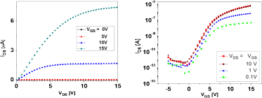
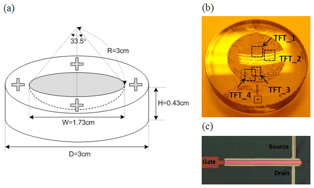
Various approaches have been proposed to realize functional devices on non-planar or hemispherical surfaces. However, those approaches are not desirable to realize highly integrated and complex device structures and circuits due to deformation, lack of scaling capability, and poor level-to-level alignment accuracy. To circumvent these limitation, we demonstrated the design and fabrication method for amorphous silicon thin-film transistors (a-Si:H TFTs) on a non-planar substrate using maskless laser-write lithography (LWL). Level-to-level alignment with a high accuracy (± 2µm or less) is achieved using LWL method. Figure below shows the output and transfer characteristics of fabricated a-Si:H TFT (W/L = 300/10).
The obtained results show that it is possible to fabricate the a-Si:H TFTs and complex circuitry on a curved surface, using a well-established a-Si:H TFT technology in combination with the maskless laser-write lithography, for hemispherical or/and non-planar imager applications. This work was done in collaboration with the Fraunhofer Institute for Applied Ophics (Jena, Germany) and is supported by DARPA/MTO HARDI Program.

 Various approaches have been proposed to realize functional devices on non-planar or hemispherical surfaces. However, those approaches are not desirable to realize highly integrated and complex device structures and circuits due to deformation, lack of scaling capability, and poor level-to-level alignment accuracy. To circumvent these limitation, we demonstrated the design and fabrication method for amorphous silicon thin-film transistors (a-Si:H TFTs) on a non-planar substrate using maskless laser-write lithography (LWL). Level-to-level alignment with a high accuracy (± 2µm or less) is achieved using LWL method. Figure below shows the output and transfer characteristics of fabricated a-Si:H TFT (W/L = 300/10).