Advanced Amorphous Silicon Thin-Film Transistor Structure
Alex Kuo, T.K. Won, and Jerzy Kanicki

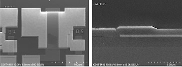
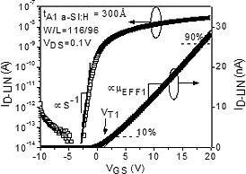
In this project we studied the intrinsic and extrinsic electrical characteristics of advanced amorphous silicon thin-film transistor (a-Si:H TFT) structure with dual amorphous silicon nitride (a-SiNX:H) and a-Si:H layers. First and second layer is deposited at higher and lower rate, respectively. The thickness effect of the high electronic quality a-Si:H film on the transistor’s electrical property was investigated; with increasing film thickness, both field-effect mobility and subthreshold swing show improvement and the threshold voltage remain unchanged. However, the source/drain contact resistance increases with the a-Si:H film thickness. This advanced a-Si:H TFT exhibits comparable electrical characteristics to conventional single channel layer TFT’s, but it can be used in manufacturing of the AM-LCD’s and AM-OLED’s due to its higher production throughput.  Based on our investigation, the film thickness of the a-Si:H film located at the channel interface should be near 300Ǻ for the TFT to exhibit adequate electrical characteristics. Such device has a linear regime field-effect mobility of 0.94 cm2 V-1 sec-1, threshold voltage of 1V, subthreshold swing of 0.51V/dec, and minimum source/drain contact resistance of 66kΩ. The advance TFT shows adequate electrical and thermal stability: the transistor’s maximum threshold voltage shift is only 4V after 10,000 sec stress at 80°C and stress current of 5.5μA. This work is done in collaboration with AKT America Inc, and is partially supported by Applied Materials Corp. Based on our investigation, the film thickness of the a-Si:H film located at the channel interface should be near 300Ǻ for the TFT to exhibit adequate electrical characteristics. Such device has a linear regime field-effect mobility of 0.94 cm2 V-1 sec-1, threshold voltage of 1V, subthreshold swing of 0.51V/dec, and minimum source/drain contact resistance of 66kΩ. The advance TFT shows adequate electrical and thermal stability: the transistor’s maximum threshold voltage shift is only 4V after 10,000 sec stress at 80°C and stress current of 5.5μA. This work is done in collaboration with AKT America Inc, and is partially supported by Applied Materials Corp.
A. Kuo, T. K. Won, and J. Kanicki, Japanese Journal of Applied Physics, vol. 47, pp. 3362-3367, 2008.
top
|

