Amorphous Metal Oxide Semiconductor Thin-Film Transistors
Tze-Ching (Richard) Fun, Hyoung Won Baac and Jerzy Kanicki
Amorphous metal oxide semiconductor (a-MOS) is a unique material with the combined properties of glass and semiconductor. Morphologically, multiple metal ions are usually introduced into a-MOS to facilitate formation of uniform, glass like, amorphous phase. Electrically, intrinsic defects such as oxygen vacancy can act as n-type dopant in a-MOS. In order to achieve the semiconducting behavior, the formation of these defects needs to be suppressed and this is commonly done through optimization of the film compositions. Hence the film electrical properties can be tailored to match desired material requirements.
 Another special feature of a-MOS is its carrier conducting mechanism. Unlike amorphous-Si, a-MOS with the properly selecting post-transition-metal cations has shown to have electrical conduction primarily through isotropic s-orbitals. Such conducting mechanism is insensitive to bond angle variation of metal-oxygen-metal chemical bonds induced by structural randomness within a-MOS and enables a-MOS to have high field-effect mobility (>10 cm2(Vs)-1) even in amorphous phase. It also allows a-MOS to withstand physical deformation without any major changes in its electrical properties which is very desirable property for flexible electronics. Another special feature of a-MOS is its carrier conducting mechanism. Unlike amorphous-Si, a-MOS with the properly selecting post-transition-metal cations has shown to have electrical conduction primarily through isotropic s-orbitals. Such conducting mechanism is insensitive to bond angle variation of metal-oxygen-metal chemical bonds induced by structural randomness within a-MOS and enables a-MOS to have high field-effect mobility (>10 cm2(Vs)-1) even in amorphous phase. It also allows a-MOS to withstand physical deformation without any major changes in its electrical properties which is very desirable property for flexible electronics.
Among various a-MOS materials, we choose for our research amorphous InGaZnO4 (a-IGZO). Similar to most conducting metal oxides, InGaZnO4 has a wide band-gap (~3.2eV) and is transparent to visible light photon energies. A-IGZO has complex crystal structure including InO2 layers inter-stack with GaZnO2 double-layers. Within GaZnO2 layers, Zn and Ga randomly occupy the same crystal sites. Because it contains heavy post-transition-metal (primarily In), a-IGZO has a high electron mobility due to the large s-orbitals overlap. The existence of Ga in a-IGZO helps in suppressing an excess of electrons. Therefore, compared to other oxide materials, a-IGZO can be made more intrinsic and is expected to have desirable semiconductor properties for thin-film transistors (TFTs).
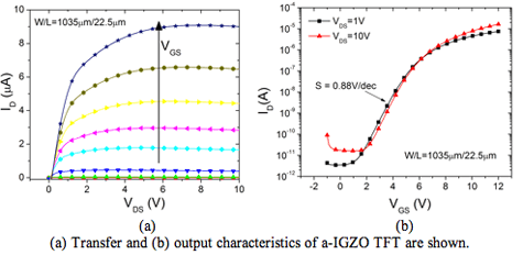
In collaboration with Prof. Hideo Hosono and Dr. Kenji Nomura of the Tokyo Institute of Technology (Japan), we studied the fundamental a-IGZO TFT electrical properties on simple inverted staggered TFT structure. Device is composed of n++Si substrate (gate), thermal SiO2 layer (gate insulator), a-IGZO channel layer and top gold electrodes (source / drain). Examples of a-IGZO TFT output and transfer  characteristics are shown below. The experimental result shows that 10~12 volt supply voltage is sufficient for a-IGZO TFT operation. Such operating voltage is significantly smaller in comparison to required gate voltage for a-Si:H TFTs (~20 to 30V). The device also shows switching properties comparable to a-Si:H TFT with a low off-current (10-11~10-12 A) and a high on/off current ratio (on the order of 106). The field-effect mobility and threshold voltage range from 0.8 to 10 cm2V-1s-1and from 1 to 5V, respectively. These device electrical properties are very desirable for future flat panel displays. characteristics are shown below. The experimental result shows that 10~12 volt supply voltage is sufficient for a-IGZO TFT operation. Such operating voltage is significantly smaller in comparison to required gate voltage for a-Si:H TFTs (~20 to 30V). The device also shows switching properties comparable to a-Si:H TFT with a low off-current (10-11~10-12 A) and a high on/off current ratio (on the order of 106). The field-effect mobility and threshold voltage range from 0.8 to 10 cm2V-1s-1and from 1 to 5V, respectively. These device electrical properties are very desirable for future flat panel displays.
By properly optimizing material composition trough deposition conditions, a-IGZO thin film can be formed at low temperatures without thermal treatment which makes it very desirable for applications that require tight thermal budget. The TFTs have also been fabricated on transparent substrates to study its optical properties. Over 80% of optical transmittance in visible range (400nm~700nm) has been observed. It implies that by utilizing a-IGZO TFT, new transparent electronics and optoelectronics could be manufactured over flexible transparent plastic substrates. The long term goal of this project is to optimize device structure for improved electrical performance, study device working principle by applying quantum mechanical and device simulation methods, and to develop a-IGZO TFT-based circuits for different applications.

top
|

