EECS 373 Lab 3: Introduction
to Memory Mapped IO
Copyright © 2010-2011,
Matt Smith,
Thomas Schmid,
Ye-Sheng Kuo,
Lohit Yerva,
and Prabal Dutta.

9/27/2011v4
Schedule
See posted lab schedule for due dates, in-lab, and post-lab due dates.
Objectives
In Lab 2 we provided you with the "hardware" to read and write the LEDs
and switches from software. We used dedicated hardware that
Actel provides for this purpose. In this lab we will discover how to
create our own hardware in the FPGA for this purpose. You will provide
the memory locations (registers), data path and control to access
registers connected to the LEDs and switches.
Overview
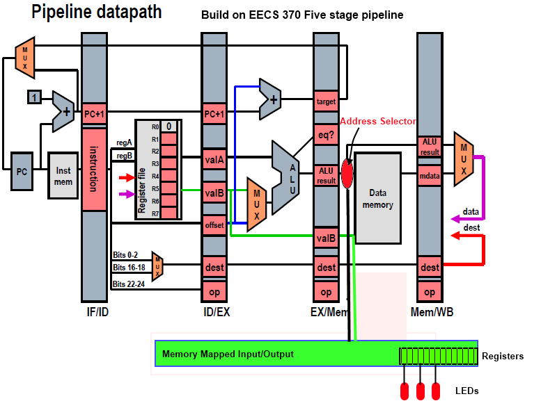
Remember the EECS 370 five stage pipeline? The only thing it could do
was read and write from memory. In EECS 270, you built a D-Flip-Flop
from gates and understood how to read and write from it. A DFF is also
called register, which is physically the same at the registers in the
processor. In the EECS 270 lab, you connected an LED to the output of a
DFF or register. How does a processor control an LED? By writing values
to the LED register. We use a method called Memory Mapped I/O to allow
the processor to access the LED register. Basically, some region of the
memory address space is allocated for the external I/O devices. The
value that the processor thinks is sending to some location in standard
memory is physically redirected to a an array of registers.
Pre-Lab Assignment
There is no Pre-Lab assignment for this lab. Read over the In-Lab
assignment and get started.
In-Lab Assignment
The In-Lab assignment is a tutorial that shows you how to interface to
the LEDs and push button
switches as memory mapped IO (MMIO), that is we will read and write the
LEDs and switches as though they are memory locations. The functional
components of the MMIO interface are organized a bit like this.
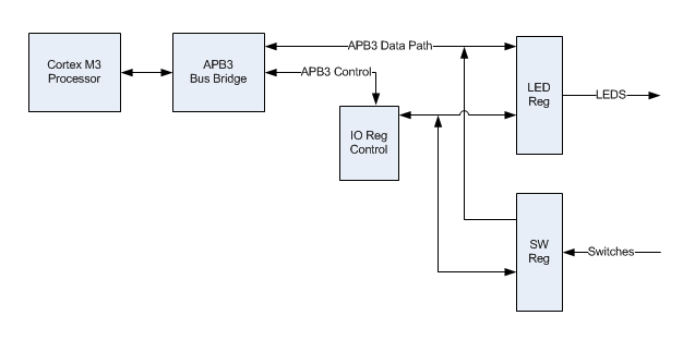
We will implement the register
control, registers, connections to
the LEDS and switches in Verilog.
We will use some prepackaged "core" from Actel and the Libero Smart
Design environment to make the bus connections.
1 Creating the IO
Registers
We will create registers in the FPGA that will act as the storage
element for the memory mapped IO
interface. Lets start with LED register. The register will be 8 bit,
read/write with the output ported directly to the LEDS. A reset is
provided that sets the register to logical 0. We have provided you with
the following example code to do this. Create a new project, create a
new Verilog file as you did in lab one and copy the the following
contents into it. Save the file. Do a HDL check to be sure all is well.
// ledreg.v

module ledreg( clk, nreset, wr_en, rd_en, data_in, data_out, led_port);

//Inputs Declarations
input clk; //Clock
input nreset; //active low reset
input wr_en; //Write Enable
input rd_en; //Read Enable
input [7:0] data_in; //Data Input

//output Declarations
output [7:0] data_out; //Data Output
output [7:0] led_port; //path to led connection

//reg Declarations
reg [7:0] ledioreg; //the io register
reg [7:0] data_out; //Data Output
wire [7:0] led_port;

//map led register to leds
assign led_port = ledioreg;

//read led register
always @(posedge clk, negedge nreset)
 begin : READ_GEN
 if(nreset == 1'b0)
 begin
 data_out <= 8'h00;
 end
 else if(rd_en)
 begin
 data_out <= ledioreg;
end end

//write led register
always @(posedge clk, negedge nreset)
 begin : WRITE_GEN
 if(nreset == 1'b0)
 begin
 ledioreg <= 8'h00;
 end
 else if(wr_en)
 begin
 ledioreg <= data_in;
 end
end
endmodule
Next lets create a register for the switches. Although we only need 2
bits for the switches, we will create an 8 bit register, make it read
only with a direct input connection from the switches. We have provided
you with the following example code to do this. Create a new Verilog
file as you did in lab one and copy the the following contents into it.
Save the file. Do a HDL check to be sure all is well.
// swreg.v
module swreg( clk, nreset, rd_en, sw_port, data_out);

//Inputs Declarations
input clk; //Clock
input nreset; //active low reset
input rd_en; //Read Enable
input [1:0] sw_port; //path from switches

//output Declarations
output [7:0] data_out;

//reg Declarations
reg [7:0] data_out;
wire [1:0] sw_port;

//read led register
always @(posedge clk, negedge nreset)
begin : READ_GEN
 if(nreset == 1'b0)
 begin
 data_out <= 8'h00;
 end
 else if(rd_en)
 begin
 data_out[0] <= sw_port[0];
 data_out[1] <= sw_port[1];
 end
end
endmodule
2 Creating and APB3
"wrapper"
The name wrapper is a bit of misnomer: it is really an interface.
Specifically, it is the Verilog that provides the interface interface
between your IO register and the APB3 bus. The wrapper provides a
control and data path conections and control logic between the IO
register and the Cortex M3 APB3 bus. The APB3 bus (advanced peripheral
bus) is designed to interface with slow IO and has a simple protocol.
Transfers fundamentally consists of two cycles: the setup phase and
access phase. During the setup phase, the processor provides unique
information that identifies the transaction such as read/write, device
address, etc. During the access phase, the device either provides or
excepts data from the processor. Additionally, the device provides a
control signal during the access phase to the processor to extend the
phase if more time is needed to latch or provide data. For more detail,
you can see the reference at the end of the lab. For your convenience,
the read/write transfer cycles with and without extended accesses are
provide below. A description of the signals follows.
 A
quick summary of the APB3 signals:
A
quick summary of the APB3 signals:
PCLK: The
bus clock. All transfers are synchronized to this clock.
PSEL:
A signal provided by the APB3 bus interface that is used to
uniquely select the device over
some predefined address range.
PADDR:
Used to address within the predefined address range.
PWRITE:
Determines if it is a read
(low) or write cycle (high).
PENABLE:
Identifies the access phase.
PREADY:
Signal used by peripheral to extend access phase. Low extends
the cycle, high releases the cycle.
PWDATA
and PRDATA: Write and read
data buses.
PSLVERR:
Use by the peripheral to indicate a transfer error.
How
can we use these transactions to read and write our IO registers?
- Consider the case of writing
the LED register. Examining the verilog
code we see that the register is written on the rising edge of clk and
wr_en true. To generate wr_en signal, the device has to be selected
(PSEL == 1), it has to be a write cycle (PWRITE == 1) and it should be
an access phase (PENABLE == 1).
- So
we have wr_en = PSEL && PWRITE &&
PENABLE with the
PCLK used as the register clock.
The read register is similarly accessed except PWRITE == 0 and the
processor requires that the data
is available at the beginning of the access cycle so PENABLE is
omitted.
- So we have wr_en = PSEL &&
!PWRITE with the PCLK used
as the
register clock.
- There is no need to extend the access
cycle, so PREADY is set logical
1. There is no criteria for PSLVERR so it is driven logical 0.
The following code is working Verilog
APB3 wrappers for the LED and
switch registers. Notice that these wrappers port some the APB3 signals
to the user IO so we can observe them. Create Verilog files, copy this
code and verify with the HDL checker.
// ledregwrp.v
module ledregwrp(
 PCLK,
 PENABLE,
 PSEL,
 PRESERN,
 PWRITE,
 PREADY,
 PSLVERR,
 PWDATA,
 PRDATA,
 LEDCON,
 TPS);

input PCLK,PENABLE, PSEL, PRESERN, PWRITE;
input [7:0] PWDATA;
output [7:0] PRDATA, LEDCON;
output PREADY, PSLVERR;
output [4:0] TPS;//test points

wire rd_enable;
wire wr_enable;

assign wr_enable = (PENABLE && PWRITE && PSEL);
assign rd_enable = (!PWRITE && PSEL); //Data is ready during first cycle to make it availble on the bus when PENABLE is asserted

ledreg ledreg_0 (.clk(PCLK), .nreset(PRESERN), .wr_en(wr_enable),
 .rd_en(rd_enable), .data_in(PWDATA), .data_out(PRDATA), .led_port(LEDCON));

assign PREADY = 1'b1;
assign PSLVERR = 1'b0;

assign TPS[0] = PCLK;
assign TPS[1] = PWRITE;
assign TPS[2] = PSEL;
assign TPS[3] = PENABLE;
assign TPS[4] = PREADY;

endmodule
// swregwrp.v
module swregwrp(
 PCLK,
 PENABLE,
 PSEL,
 PRESERN,
 PWRITE,
 PREADY,
 PSLVERR,
 PWDATA,
 PRDATA,
 SWCON,
 TPS);

input PCLK,PENABLE, PSEL, PRESERN, PWRITE;
input [7:0] PWDATA;
input [1:0] SWCON;
output [7:0] PRDATA;
output PREADY, PSLVERR;
output [4:0] TPS;//test points

wire rd_enable;
wire wr_enable;

assign rd_enable = (!PWRITE && PSEL); //Data is ready during first cycle to make it availble on the bus when PENABLE is asserted

swreg swreg_0 (.clk(PCLK), .nreset(PRESERN),
.rd_en(rd_enable), .data_out(PRDATA), .sw_port(SWCON));

assign PREADY = 1'b1;
assign PSLVERR = 1'b0;

assign TPS[0] = PCLK;
assign TPS[1] = PWRITE;
assign TPS[2] = PSEL;
assign TPS[3] = PENABLE;
assign TPS[4] = PREADY;

endmodule
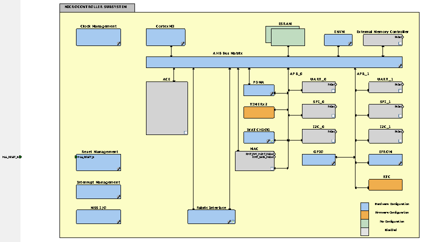
3 Provide
Microcontroller Subsystem Components
To complete the connection between the IO
registers and APB3 bus, we
will need access to the system power up reset, a clock for the bus and
connections to the APB3 data and control path. Access to these
connections is provided thru the SmartFusion MSS (Microcontroller
Subsystem). Many standard microcontroller subsystem components are
provided including general purpose timers, serial IO interfaces, memory
controllers, etc. These components are configured under the MSS
(Microcontroller Subsystem) icon.
3.1
Enable Relevant MMS
Components
Double click on the MSS icon in the
project flow window and provide a
name to the MSS configure such as m. A view of the MSS system
will open revealing all the available components and connections. All
the components are enabled to begin. We will only need the Reset
Management, Fabric Interface< Watch Dog and Clock Management
Component. The components are enabled by selecting the check box in the
lower right corner. Notice that some components like the Clock
Management do not have the option to exclude since they are needed for
any configuration. Turn off all the components we don't need and your
canvas should look something like this.
3.2
Configure Clock
Manager
This component provides clock sources for
the various system components
and custom FPGA hardware. We will use a clock that can be mapped to the
FPGA hardware for the APB3 bus clock. Double click on the Clock
Management icon. FAB_CLK (fabric clock) is the FPGA clock. Enable by
clicking on the box. We are going to divide the clock down from the
source clock (100 MHz) to 25 MHz. Do this by selecting the drop down
menu just upstream from the FAB_CLK output and select divide by 4. The
default source clock should be the RC oscillator (upper left). Also,
you should notice the FAB_CLK added as an output port (upper right)
from the MSS system to the FGPA fabric when you return to the MSS
canvas. The connections are not shown between the components and MSS
boundary. You can add them under the Canvas menu if you wish (show
nets). The clock manager configuration should look something like this
before closing.
3.3
Configure Reset
Manager
The reset manager provides power up
system reset to the various
components and FPGA fabric. We need provide the power up reset to the
FPGA fabric. Open the Reset Manager and select "Enable MSS to Fabric
Reset". It should look like this and you should notice a reset output
to the FPGA fabric on the MSS canvas.
3.4
Configure Fabric
Interface
The Fabric Interface component is use
configure bus ports to custom
FPGA hardware. In this case we must configure a APB3 interface. Double
click on the icon opening the fabric interface configuration. Notice
that the MSS clock frequency and fabric clock frequency are inherited
from the clock settings. We need a APB3 interface so select "AMBA
APB3". The interface will act as a "Master" controlling the LED and
switch registers so configure as MSS Master. The setting should look
like this.
3.5
Generate MSS
Finally HDL has to be generated from the
MSS for synthesis. Click the
generate icon or select under the design menu. Make sure there are no
errors indicated in the script below. The MSS generator will warn you
that a root has not been set for the design hierarchy. You can ignore
this for now. The final canvas should look something like this with the
net view enabled (not necessary). Inspect the project explorer in the
files tab and you will see Verilog files added for the MSS components.
4 Connecting the IO
Register Wrappers to the APB3
Libro provides a graphical editor for making system component
connections between MSS components, custom logic and other high level
core. We will use this tool to make our connection between the IO
register wrappers and the Cortex M3 APB3 bus. Open SmartDesign (click
on the ICON in Project Flow), select SmartDesign Component, choose a
descriptive name such as apb3_to_ledswreg. A canvas should open without
any components.
4.1
Set Design Hierarchy
Root
Select the Hierarchy tab in the Design Explorer, select the
apb3_to_ledswreg, right click and set as the root. This sets the
apb3_to_ledswreg as the top level in the design hierarchy. The file
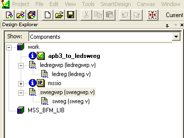
hierarchy should look something like this. Notice IP from the MSS
configuration and the verilog files we provided earlier.
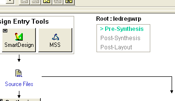
 Notice that in the design flow apb3_to_ledswreg is set as the
root in
the upper right corner.
Notice that in the design flow apb3_to_ledswreg is set as the
root in
the upper right corner.
4.2
Instantiate MSS
Components in SmartDesign Canvas
We need to start by instantiating the MSS
components we establishes
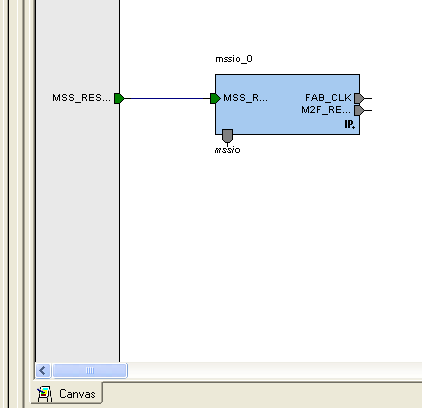
earlier in the SmartDesign Canvas. Select IP mssio in the Design
Explorer and drag it into the SmartDesign canvas. Or, select IP mssio,
right click and choose instantiate in apb3_to_ledswreg. The MSS
components we configured will be represented as a block with the ports
we provided. The reset connection is automatically made since this is a
fixed input. The block should look something like this.
4.3
Instantiate
Register APB3 Wrappers in SmartDesign Canvas
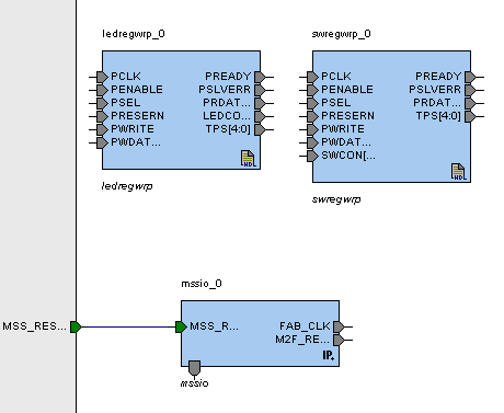
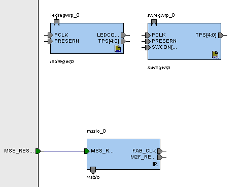
Again, select the ledregwrp and swregwrp and drag onto the
canvas. The
blocks will be instantiated and look a bit like this.
4.4
Convert IO Register
APB3 Wrapper Ports to APB3 Slave
Interface
Next we need to repackage the
wrapper ports so that they interface a
bit easier with standard APB3 signals. SmartDesign has a handy tool for
this. Select the Bus Definitions tab (lower right) in the Catalog
window (right). Select APB, AMBA, AMBA2, slave. Drag this onto one of
the instantiation blocks of one of the wrappers. You will be prompted
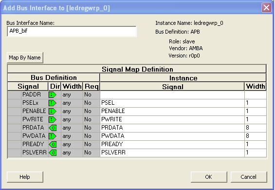
to associate the signals of the wrapper with standard APB3 signals.
Many of these can be associated automatically by using the map by name
feature (upper right) if we took care to use similar names when we
created the wrapper ports. You will find most of these signals mapped
except PSELx and PADDR. Use the signal window set PSELx to PSEL and the
width window to set to 1 bit. We are not using PADDR so it can remain
blank. The result should look like this.
 Repeat the process for the other wrapper. The blocks should now
look
like this. Notice that all the APB3 signals are contained in one bus
connection.
Repeat the process for the other wrapper. The blocks should now
look
like this. Notice that all the APB3 signals are contained in one bus
connection.
4.5
Instantiate APB3
Core Interface
Under bus interfaces in the catalog
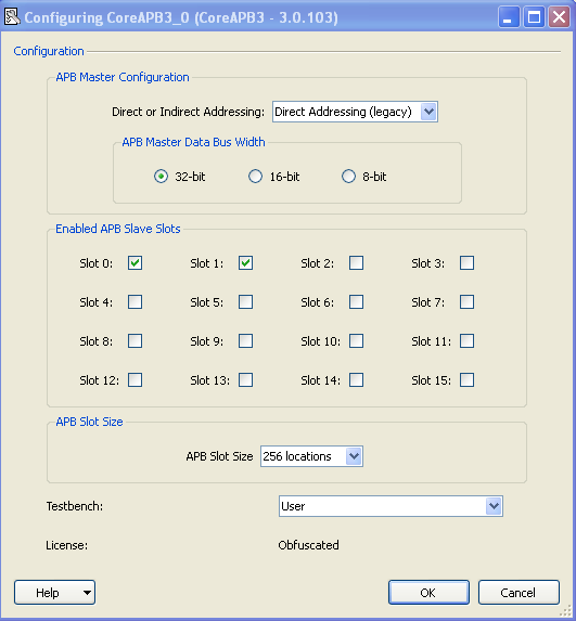
window (left) select CoreAPB3 and
drag onto the canvas. A configuration window will appear. Basically
allows you to determine how many IO devices you wish to select and how
much memory space you wish to allocate per device. Keep all the
settings but reduce the slot number (devices) to just two. It should
look like this.
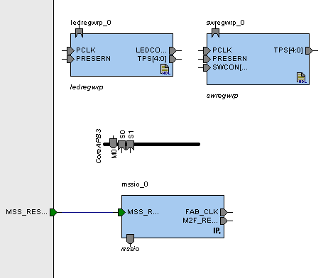
 Acknowledge this window and a APB3 bus connection icon will
appear in
the canvas. You may want to position it and size it. The canvas should
look like this now.
Acknowledge this window and a APB3 bus connection icon will
appear in
the canvas. You may want to position it and size it. The canvas should
look like this now.
4.6
Connect IO Register
APB3 Wrappers to APB3 Core Interface
Finally, we can connect the components. SmartDesign has a handy
tool
for this to. Right click on the canvas and select auto connect. A
window will appear asking you to acknowledge the addresses SmartDesign
is assigning to the 2 registers. Notice that each address has an
address range of 256 bytes as set in the configurator earlier. Agree to
these addresses. The window looks a bit like this.
 After acknowledging the memory locations the APB3 connections
will be
made and look a bit like this.
After acknowledging the memory locations the APB3 connections
will be
made and look a bit like this.
4.7
Connect Resets
Although the PCLK and FAB_CLK have different names, the tool
assumed you
wanted to connect these. In this case it is what we intended, but be
careful when using the auto connect and be sure the connections are
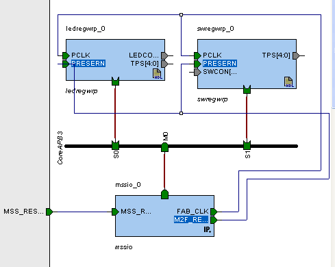
correct. The reset will have to be connected manually. We need to
connect the fabric reset output from the MSS block to the preset inputs
of the register wrappers. To connect two ports or more ports, select
all the ports to be connected (control, shift, click). Right click over
one of the selected ports and select connect. The canvas will no show
the connection.
 Notice that the components are all
located to one side of the canvas
and the reset connection has to be routed over one of the components.
SmartDesign has an auto component arrange feature to nicely distribute
the components. Right click in the window and select auto arrange
instances. Usually this works, but you might have to manually adjust
too. Also use the auto fit feature after auto arranging. It is this
middle icon.
Notice that the components are all
located to one side of the canvas
and the reset connection has to be routed over one of the components.
SmartDesign has an auto component arrange feature to nicely distribute
the components. Right click in the window and select auto arrange
instances. Usually this works, but you might have to manually adjust
too. Also use the auto fit feature after auto arranging. It is this
middle icon.
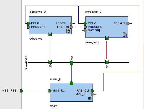
 Here is what happened to the above canvas after auto arranging.
4.8
Connect LEDs, Switch
Ports and Test Points
Finally we need to connect the LEDs,
Switches and Test Points to the
appropriate FPGA pins. Since the test points are identical for both
wrappers we need only connect one set. You can add FPGA ports to the
canvas by right clicking just outside the canvas and selecting add
port. However, when you have an existing port on the canvas there is a
much easier way. Select the port you wish to provide connection to,
right click and select promote to top level. This will create the
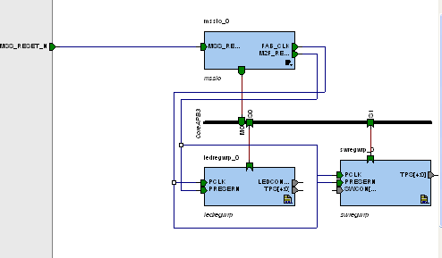
connection automatically. After adding these connections and auto
arranging instances the canvas should look like a bit like this.
4.9
Check Design and
Generate HDL for Synthesis
Before synthesis these graphical components need to be converted
to
HDL. Before doing so, we will run design check. It is the left icon
here.
 You will notice that the set of unconnected test points are indicated
as floating or unconnected. This is fine since we did it intentionally.
Next generate HDL by selecting the right icon here.
One warning about the unconnected test points should be indicated. You
should see new verilog under the apb3_to_ledswreg icon in file view of
design explorer.
You will notice that the set of unconnected test points are indicated
as floating or unconnected. This is fine since we did it intentionally.
Next generate HDL by selecting the right icon here.
One warning about the unconnected test points should be indicated. You
should see new verilog under the apb3_to_ledswreg icon in file view of
design explorer.
5 Synthesize all
Components
Synthesize all the components like we did in lab 1 by selecting the
Synthesis icon and Running. Correct any errors that might occur. Before
we can synthesize, you must go back to the MSS configuration and
generate design again. If this is closed, you can open by clicking on
the icon in the hierarchy view in design explorer. If you don't do
this,
you will get a cryptic error from the Synopsis indicating that there is
an error and it can't synthesize.
6 Assign FPGA Pins
Assign FPGA pins to the LEDS, switches and Test Points like you did in
lab1. You can ignore the MSS_Reset and just leave it unassigned. It
will be automatically assigned to a fixed pin.
7 Place and Route
Run place and route like you did in lab 1.
8 Simulation
While it is possible to simulate the APB3 bus, we will skip this step
for now and verify on the kit.
9 Program FPGA
Program the FGPA like you did in lab 1.
10 Debug and Verify with
SoftConsole
We will use SoftConsole and the debugger to verify the operation of the
IO registers. We will use some GDB read/write commands via the
SoftConsole debugger connection to verify the operation of the
registers. We will also observe some of the APB3 bus control signals
with the scope.
10.1
Create a
SoftConsole Project and Debugger Session
Open SoftConsole and create an assembly project like you did
in lab 2. Use the infinite loop assembly example from lab 2.
Remember to include the link file and provide all the settings
under project-->properties. Open a debuging session
via SoftConsole as you did in lab 2.
10.2
Use GDB Commands to
Verify IO Register Function
GDB provides some basic read/write commands for accessing memory. We
could do this thru the command prompt, but we would have to go thru all
the setup you experienced in lab 2. Once the debug connection is open
in
SoftConsole, you can type any GDB command in the console window at the
bottom in Debug view.
10.2.1
Write the Led Register
The debugger in SoftConsole must
be paused for these commands to work.
The GDB command to write a register is
"set".
set
*(type *) address = contents
type
is
char, halfword or word
address
is location contents
is value to be written
When we setup the APB3
interface we discovered that register base
address was 0x40050000. Although the register is 8 bits, it
can be treated like a 32 bit value with the low order byte effective.
For example,
set *(int *) 0x40050000 = 0x55
Try writing different values
and see if the LEDs correspond to your values.
10.2.2
Read the Switch Register
The GDB command to read is
examine or simply "x". The format is:
x
address
address
is the memory location to read The default data
type is a 32 bit value
When we setup the APB3
interface we discovered that register base
address was 0x40050100. Although the register is 8 bits, it
can be
treated like a 32 bit value with the low order byte effective. For
example,
x 0x40050100
Try reading different
values and see if it corresponds to the switch
values. Remember
the switches are active low.
There are many other options
for the examine command. You can search the web for GDB quick
references for more detail.t
10.3
Use GDB Commands to
Observe the APB3 Bus Signals
Lets observe some basic APB3 bus operation with the scope. We ported
the
following signals with our Verilog code.
USER IO 1 = PCLK
USER IO 2 = PWRITE
USER IO 3 = PSEL
USER IO 4 = PENABLEUSER
USER IO 5 = PREADY
Note, it may be necessary to
power reset the kit to get the FAB clock
and in this case the APB3 clock set. You can try the RESET button or it
may be necessary to disconnect the USB power cable (nearest push
button). This will disrupt the SoftConsole debug connection. You need
to reload the configuration to recover the connection. Click on the
following icon (upper left) in the debug window and reload the
configuration

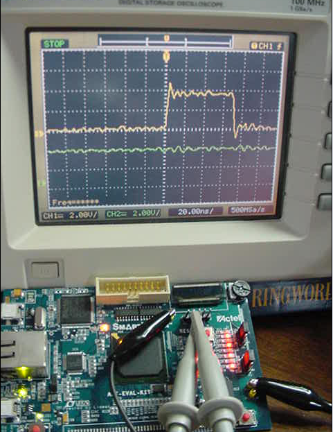
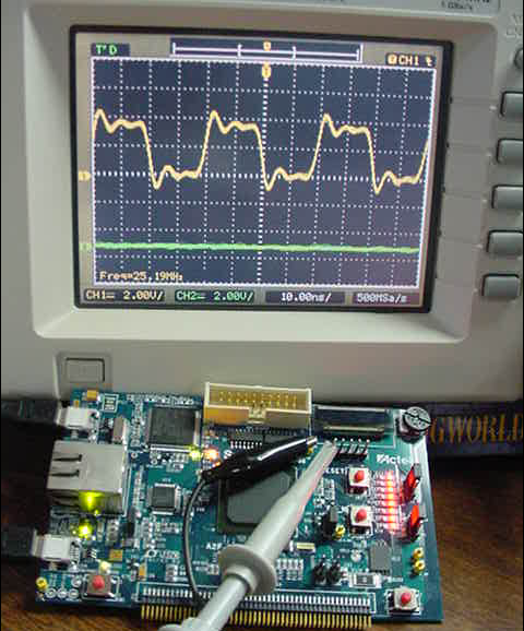 PSEL or peripheral select determines if the register is selected. Lets
monitor this signal and trigger on it going from low to high. It will
only last for one access so set the trigger up for single sweep. Use
the LED register access command:
set *(int *) 0x40050000 = 0x55
Attach the clock output to channel 2. Execute the command and see if
you can capture it on the scope. It should look like this.
PSEL or peripheral select determines if the register is selected. Lets
monitor this signal and trigger on it going from low to high. It will
only last for one access so set the trigger up for single sweep. Use
the LED register access command:
set *(int *) 0x40050000 = 0x55
Attach the clock output to channel 2. Execute the command and see if
you can capture it on the scope. It should look like this.
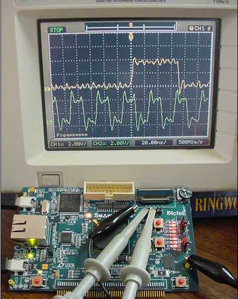 Notice that PSEL starts just after the rising edge of clock and last
for about 2 clock periods as indicated in the timing diagrams above.
Keep PSEL on channel one, but put probe 2 on the PENABLE. Again trigger
as above. It should look something like this.
Notice that PSEL starts just after the rising edge of clock and last
for about 2 clock periods as indicated in the timing diagrams above.
Keep PSEL on channel one, but put probe 2 on the PENABLE. Again trigger
as above. It should look something like this.
 Notice that PENABLE lasts for one clock period during the access phase
(2nd clock cycle) as shown in the timing diagrams above.
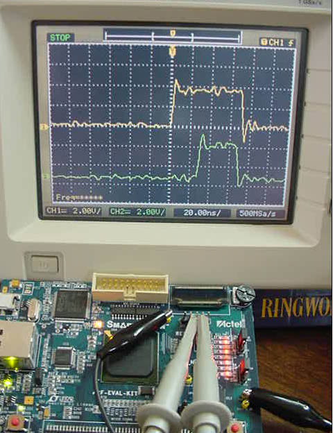
Keep PSEL on channel one, but put probe 2 on the WRITE line. Notice it
stays active (logical high) for the duration of both setup and access
cycles.
Notice that PENABLE lasts for one clock period during the access phase
(2nd clock cycle) as shown in the timing diagrams above.
Keep PSEL on channel one, but put probe 2 on the WRITE line. Notice it
stays active (logical high) for the duration of both setup and access
cycles.
 Keep the scopes connected as in the previous step, but this time try
executing the read command to the switch register.
x 0x40050100
Notice that the scope does not trigger. The PSEL that is ported on this
test point is from the LED register. It must not respond to a switch
access! If you wish to observe the PSEL for the switch register we
would have to go back and port it in SmartDesign to a user IO pin.
Keep the scopes connected as in the previous step, but this time try
executing the read command to the switch register.
x 0x40050100
Notice that the scope does not trigger. The PSEL that is ported on this
test point is from the LED register. It must not respond to a switch
access! If you wish to observe the PSEL for the switch register we
would have to go back and port it in SmartDesign to a user IO pin.
10.4
Write a Simple
Program
Lets write a simple program that reads the switches and writes the
LEDs. The program simply reads the switches and ports them to two of
the LEDs.
Assembly and Link this code. Set up a Debug connection and try the
code.
.equ STACK_TOP, 0x20000800

.equ LEDIO_REG_BASE, 0x40050000
.equ SWIO_REG_BASE, 0x40050100

	.section .int_vector,"a",%progbits @ First linker code section
	.global _start @ Linker entry point
_start:
	.word STACK_TOP, main
	@ End of int_vector section

	@ Standard text section
	.text
	.syntax unified
	.thumb

	.type main, %function
main:
	@ Load led register base address
	movw r0, #:lower16:LEDIO_REG_BASE
	movt r0, #:upper16:LEDIO_REG_BASE
	@ Load switch register base address
	movw r1, #:lower16:SWIO_REG_BASE
	movt r1, #:upper16:SWIO_REG_BASE

loop:
	@ Read switch register
	ldr r3, [r1, #0]
	@ Write switch values to led register
	str r3, [r0, #0]
b loop
.end
Try running the code and observing PSEL and PENABLE. You will notice
you do not have to single sweep trigger since the writes are triggering
at a regular rate.
Lab 3 Debugging Pit Falls
1) You have to stop or pause the debugger to use
FlashPro.FlashPro will not indicate a fault, but the kit will not be
identified when FlashPro starts.
2) Sometimes when running the debugger things just hang. Try reloading
the debug session or you may have to press the RESET switch on the kit.
3) If you change the settings for the FAB clock and reprogram the FPGA,
it may be necessary to power reset the kit for new FAB clock setting to
work. Disconnect the USB power cable (nearest push button) and
reconnect. This will disrupt the SoftConsole debug connection. You need
to reload the debug configuration to recover the connection.
Post-Lab Assignment
The Hardware Assignment
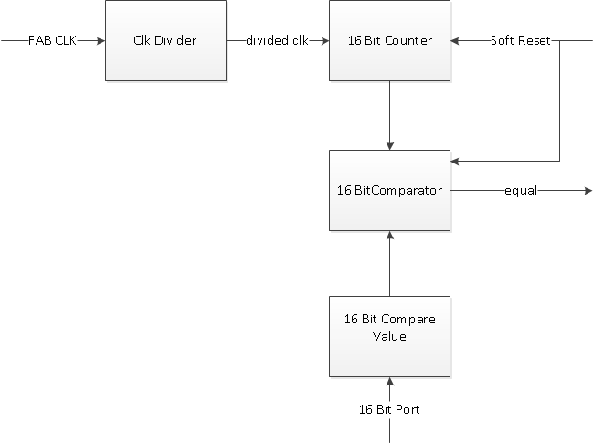
For the post lab, you will add a timer to your In-Lab hardware that can
be used by the softare via memory mapped IO registers. The timer will
count at a 100Hz and signal "equal" when a count value is
reached (Compare value == Counter value). Application software can
use the timer to provide delays
by
writing an compare value to the timer and then monitoring a status
equal bit
until the counter reaches the compare value . For example, to provide a
delay of 1 second, write a value of 100 to the compare value. A soft
reset must be
provided by the user to reset the counter and equal status bit to zero.
A
functional block
diagram follows.
Application Details
The
timer uses the FAB CLK as a source clock and must reduce it to
approximately 100 Hz. The
divided clock is used to source
a 16 bit counter. When the counter value and compare value are equal,
the comparator provides a signal "equal" indicating the value is
reached.
The value is held until a external reset value (soft reset) is
provided.
// timer.v
module timer (clock, compare, equal, soft_reset);
input clock;
input [15:0]compare;
input soft_reset;
output equal;

reg [15:0] counter, ncounter;
reg equal;
wire divided_clock;
reg [17:0] divide;
reg [17:0] nextDivide;

wire [15:0]nextcounter = counter + 16'd1;

//The following code divides the fabric clock to approximately 100Hz

always @*
  begin
      nextDivide = divide + 16'd1;
  end

always @(posedge clock)
begin
    divide <= nextDivide;
end

assign divided_clock = divide[17];

// This code provides the counter, comparator and software reset functions
of the timer
always @*
begin
    if (soft_reset == 1)
	begin
		equal = 0;
	end
	else if (counter == compare)
	begin
		equal = 1;
	end
	else
	begin
		ncounter = counter + 1;
	end
end

always @(posedge divided_clock or posedge soft_reset)
if (soft_reset)
begin
    counter <= 0;
end
else
begin
	counter <= ncounter;
end

endmodule
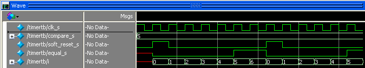
Functional Simulation of Timer Verilog
A simulation of the timer Verilog follows with the compare value set to
5. Notice that the equal value is held until reset is applied.
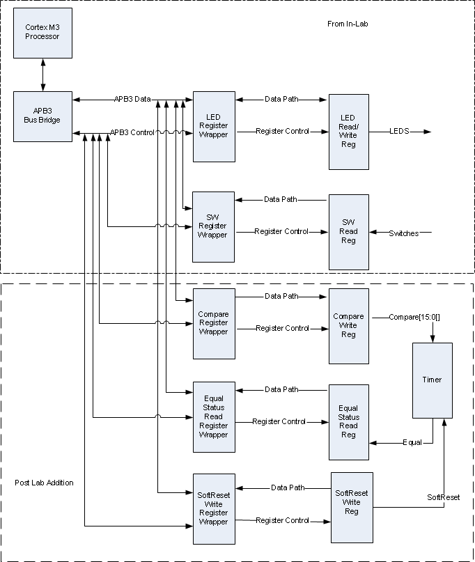
Interfacing to the APB3
The
timer can be instantiated and added to the top level canvas as a module
as you did above. The timers ports: compare, equal and soft_reset will
have to be connected to the APB3 bus via a register interface not
unlike the register interfaces provided for the switches and leds.
In this case;
however, we will provide 3 APB3 interfaced registers to support the
timer: a 16 bit write only compare register, a 1 bit read only equal
register and a 1 bit write only soft_reset register. Note, you
need to keep the switch and led registers for a software application.
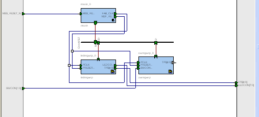
The MMIO including the timer should look a bit like this.
Soft_reset
Register Verilog
The soft reset is a software generated
reset to clear the timer counter and reset the timer equal status. The
Verilog for a Soft_reset register and
Soft_reset register wrapper follows. You will have to follow the
procedure above to instantiate the module in the top level canvas. Be
sure and connect the Soft_reset signal to the Timer module. You will
have to add another slave port the APB3 bus. Click on the
buss-->properties and add another slot.
Soft
Reset
Register
// softresetreg.v

module softresetreg( clk, nreset, wr_en, rd_en, data_in, softreset);

//Inputs Declarations
input clk; //Clock
input nreset; //active low reset
input wr_en; //Write Enable
input rd_en; //Read Enable
input [7:0] data_in; //Data Input

//output Declarations
output softreset; //path to softreset

//reg Declarations
reg [7:0] softresetreg; //the io register
wire softreset;

//map led register to leds
assign softreset = softresetreg[0];

//write softreset register
always @(posedge clk, negedge nreset)
 begin : WRITE_GEN
 if(nreset == 1'b0)
 begin
 softresetreg <= 8'h00;
 end
 else if(wr_en)
 begin
 softresetreg[0] <= data_in[0];
 end
end
endmodule
Soft Reset Wrapper
// softresetwrp.v
module softresetwrp(
 PCLK,
 PENABLE,
 PSEL,
 PRESERN,
 PWRITE,
 PREADY,
 PSLVERR,
 PWDATA,
 PRDATA,
 SOFTRESET,
 TPS);

input PCLK,PENABLE, PSEL, PRESERN, PWRITE;
input [7:0] PWDATA;
output [7:0] PRDATA
output SOFTRESET;
output PREADY, PSLVERR;
output [4:0] TPS;//test points

wire rd_enable;
wire wr_enable;

assign wr_enable = (PENABLE && PWRITE && PSEL);
assign rd_enable = (!PWRITE && PSEL); //Data is ready during first cycle to make it availble on the bus when PENABLE is asserted

softresetreg softresetreg_0 (.clk(PCLK), .nreset(PRESERN), .wr_en(wr_enable),
 .rd_en(rd_enable), .data_in(PWDATA), .softreset(SOFTRESET));

assign PREADY = 1'b1;
assign PSLVERR = 1'b0;

//for the post lab you are asked to monitor the PSELs for all the MMIO with the logic anlayzer. Choose a test point that you wish
// to port the PSEL on for each MMIO wrapper
//assign TPS[0] = PCLK;
//assign TPS[1] = PWRITE;
assign TPS[2] = PSEL;
//assign TPS[3] = PENABLE;
//assign TPS[4] = PREADY;

endmodule
Timer Counter and Equal Status
Register Verilog
Complete the Verilog for the
compare and equal registers, add to your top level canvas. Hint. Use
the LED register and LED register wrapper Verilog as a model to build
the compare register and wrapper Verilog. Similarly, look at the switch
register and switch register wrapper Verilog as a model to build the
enable register and wrapper Verilog.
The Software Assignment
Write an assembly program that uses your timer, the switches and
LEDs to:
- Blink the LEDs in sequence from top to bottom (led 0 to led 7) at
a user
determined rate.
- The starting rate should be 1Hz
- The rate should increment by 1 Hz when SW1 is pressed and
released.
- The rate should decrement by 1 Hz when SW2 is pressed and
released.
- The rates should remain between 1 and 10 Hz.
A few notes:
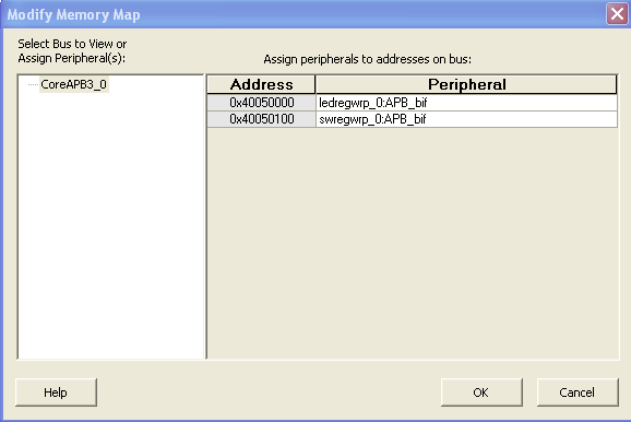
- You can get the addresses for your timer registers by selecting
the APB3 bus in the top level canvas, right clicking and selecting
memory map.
- Consider the following process to develop your software:
- Start by blinking one LED at 1 Hz using the timer.
- Add the switch control to increase the or decrease the blink
rate.
- Modify to blink the LEDs in sequence.
- To get the switches to increase or decrease the rate in steps of
1Hz, you will have to detect the change in the switch value. Just
detecting the switch level is not sufficient. Just level detection will
result in the software detecting that the switch is pressed for several
loops decreasing or increasing the rate very quickly to one of the
boundaries. To detect a transition, you will have to keep the previous
value of the switch in a memory location or spare register and detect
if the switch has changed or not.
Post Lab Deliverables
1) Provide a coy of your
assembly code.
2 ) Demonstrate the operation of your timer and software
application on or before
the due date to one of the 373 lab instructors.
3) Answers the following questions:
- Which APB3 bus signal uniquely identifies the bus transaction for
a particular device? In general terms, what bus signals are decoded to
generate this signal?
- How many wait cycles do your MMIO registers need if any?
- The timer verilog divides the fabric clock to approximately 100Hz
by using a simple binary counter. What is the actual value in Hz?
- In the timer Verilog code, what signal edge is the timer counter
set to zero on? Why do you suppose this is necessary?
You can use the Answer
Sheet to provide the dated
signature, answers to the questions and group identification.
Extra Credit
1) Port the PSELs for all your MMIO
registers to user IO pins (test
points): Switches, LEDs and Counter registers. Connect them to 5
consecutive channels on the logic analyzer. Set the logic analyzer to
trigger on the switch register PSEL . Provide a print of the logic
analyzer view showing all the
PSELs. Identify each PSEL labeling with the register name.
References