EECS 373 Lab 7: Data Converters
Copyright © 2010-2011
Ye-Sheng Kuo,
Thomas Schmid,
Matt Smith,
Lohit Yerva,
and Prabal Dutta.

11/07/2011
Schedule
EECS
373 Fall 2011 Home Page
EECS
373 Labs Google Calendar
Introduction
As you might guess, with all the other goodies included in the
SmartFusion
MSS the folks at Actel did not forget ADC and DAC resources. The MSS
ACE (Analog Computing Engine) is relatively complex
component providing DAC/ADC functionality, sampling
control, analog threshold detection, filtering and DMA access just to
mention a few. Despite this apparent complexity, the ACE can be
relatively easy to use. The ACE like the other MSS components is
automatically interfaced to the peripheral bus and a user friendly GUI
is provided for configuration. Of course, a library of drivers is also
generated.
Objectives
The purpose of this lab is to...
- Learn how to configure the ACE for basic DAC and ADC operations.
- Learn to measure ADC quantization and typical transfer function
characteristics.
- Learn the basics of sampling by observing aliasing of sampled
sine wave.
- Learn how to build a simple audio amplifier.
- Sample and record an audio signal for playback using the ACE and
your audio amplifier.
Background
ADC Quantization and Transfer Function Characteristics
Quantizing error is inherent in most measurements
and limits the certainty of measurement. The quantizing error for
an ADC
is defined to be 1 LSB. It can also be expressed in volts or LSBv for
an n-bit
ADC .
Quantizing
error in
volts = voltage range of conversion/2^n
For our converter, the voltage range is 2.56
volts. If we program the ACE to be an 8 bit ADC, the quantizing
error in
milli-volts
will be
LSBv =
2.56 volts/2^8
= 10 mv
So, you can only know the value to 10 mv. The ideal quantum size of 1 LSB
can actually
vary to be larger or smaller from fabrication issues and other sources.
These
effects are characterized as integral non-linearity (INL) and
differential
non-linearity (DNL). Under normal
conditions
in the lab you will NOT observe this.
Plotting the conversion value against the analog
value
defines the ADC transfer characteristic or input to output
relationship.
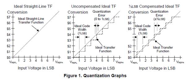
The first graph shows the ideal transfer function
excluding
quantizing effects. The second case illustrates the affect of
quantizing resulting
in a stair case like transfer function. In this case the quantization
error is
from 0 LSB to 1 LSB. The last graph illustrates an ADC model that
shifts the
transfer function to center the quantizing error over the conversion
intervals.
In this case, the quantization error is +/-
½ LSB. In both cases the
quantizing error is 1 LSB, but the relationship of the conversion value
to the
input voltage is shifted by ½ LSB.
Sampling Basics
When converting relatively stable voltages to digital values a few
samples are sufficient to represent the voltage. However, when sampling
time varying signals the question arises, just how many samples are
required
to represent the signal. The Nyquist-Shannon sampling theorem predicts
that periodic signals can be reproduced when the original signal is
sampled at >= 2 times its period. If the signal is sampled at a rate
that is less than the 2 times its period, the reconstructed signal will
have a different frequency and shape. A simple predictor is given by
the following equation:
alias frequency = sampled signal
frequency - sampling frequency
The reconstructed
signal is commonly referred to as an alias and is a common problem in
applied signal processing. There are many topics forming the foundation
of signal processing, but
these basics should cover our needs for the present.
Additional Material
Overview
Pre-Lab Assignment
- Read through the lab 7 notes.
- Read through the data converter lecture.
In-Lab Assignment
- ADC/DAC Basics
- Aliasing, Quantization error, Smoothing filter
- Simple Audio system
In-Lab Assignment
Aliasing, Quantization error
Configuring the SmartFusion ACE
For this part of the lab we will configure the ACE component in the
MSS, synthesize, Place and Route and flash the FPGA. Disable
everything but the ACE and UART_0.
Each SmartFusion
Eval Kit has 10 direct analog input channel and 2 Sigma-delta DACs. We
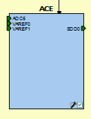
want to use just one of each. Open the Libero, SmartDesign. Double
click ACE
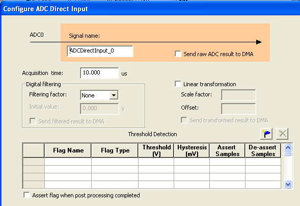
In left column, add a ADC Direct Input service. Put ADCDirectInput_0
in Signal Name and click OK. On the
top of configurator, set the resolution to 8 bits.
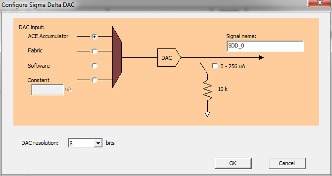
Add another Sigma Delta DAC service, select ACE Accumulator
as DAC input and
select the DAC resolution to 8 bits. Click OK.
Set your ADC Direct Input Package Pin to V12 ( ADC5 ), and
Sigma Delta DAC Package
Pin to V7 ( SDD0 )

Go to Controller tab, select only ADC1_MAIN. Add all
Available
signals to sampling rate requirement. Click Calculate Sequence and
Actual Rate
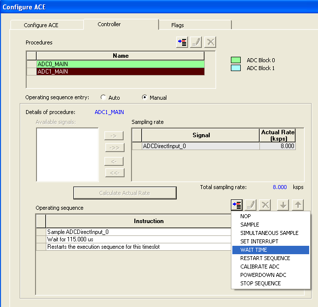
Notice that the Total sampling rate should be 87.000 ksps. We
want to slow it down to 8 ksps.
Set the Operating sequence entry to Manual and insert a
WAIT TIME
operating sequence slot, using  ,
and configure it to 115us. Move the Wait
for 115.00us above Restarts the execution sequence for this
timeslot. Click Calculate Actual Rate.
The Actual Rate for ADC / DAC should be 8.000 ksps.
,
and configure it to 115us. Move the Wait
for 115.00us above Restarts the execution sequence for this
timeslot. Click Calculate Actual Rate.
The Actual Rate for ADC / DAC should be 8.000 ksps.
Click OK and go to Firmware tab. Check the UART, GPIO, and
ACE drivers.
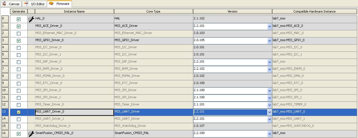
Click Save and Generate. Put the IP core to canvas and
run the synthesis, place &
route and flash your SmartFusion.
A Simple ADC/DAC Application
Create a C project in Softconsole as you did before, set the linker
script, import the drivers. The following code reads the ADC
and write the DAC with the ADC conversion value
#include <stdio.h>

#include <inttypes.h>

#include "drivers/mss_ace/mss_ace.h"

#include "drivers/mss_uart/mss_uart.h"


ace_channel_handle_t adc_handler;

int main(){
    ACE_init();

    /* DAC initialization */
    ACE_configure_sdd(
    	SDD1_OUT,
    	SDD_8_BITS,
    	SDD_VOLTAGE_MODE | SDD_RETURN_TO_ZERO,
    	INDIVIDUAL_UPDATE
    );
    ACE_enable_sdd(SDD1_OUT);

    /* handler for ADC channel */
    adc_handler = ACE_get_channel_handle((const uint8_t *)"ADCDirectInput_0");

    while(1){
    	uint16_t adc_data = ACE_get_ppe_sample(adc_handler);
    	ACE_set_sdd_value(SDD1_OUT, (uint32_t)(adc_data>>4));
    }
    return 0;
}
Put the code in a main.c file. Compile the source code and launch
the debugger session.
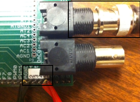
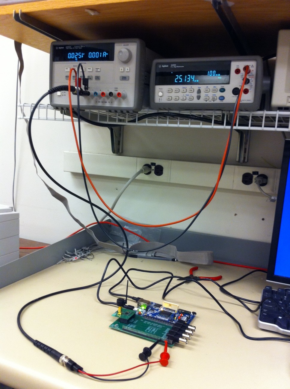
Connecting to the DAC and ADC
Hook the signal generator
to the extension board header pin 5 ( paper label) in the bottom right corner to provide
input to the ADC. If you don't have a paper label this is labeled ADC1.
Observe the DAC output on the 2nd BNC connector from the header pin.
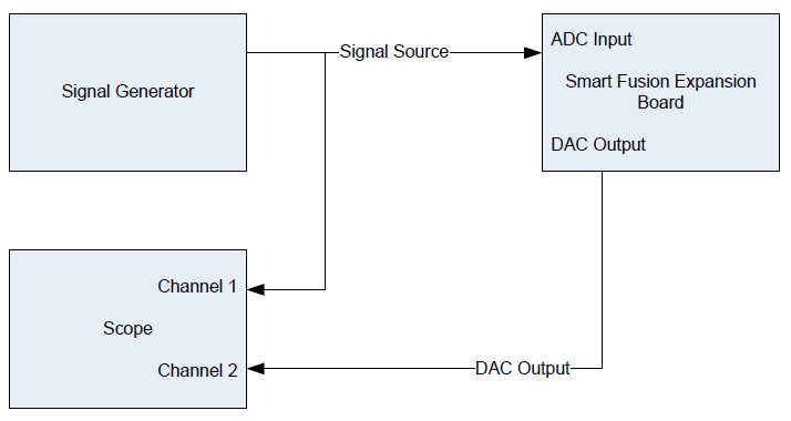
Test ADC and DAC setup
Using the signal generator as a signal source, provide a sine wave that
centers a sine wave over the input range of the ADC (0 - 2.56 volts). A
DC offset of 1.25 volts should be fine with a Vpp (peak to peak)
voltage of 2.5 volts. Be sure the signal generator output is set to
High Z to insure accurate signal levels. Verify with the scope before
attaching to the kit to avoid damage to the ACE.
Aliasing Measurements
Slowly increase the frequency of the signal generator while observing
and measuring the frequency of DAC. Determine the frequencies or
frequency ranges for the following questions. You will need this
information to answer questions in the post lab.
- Over what frequency range is the reproduced signal frequency (DAC
output) and signal shape visually reproduced well?
- Over what frequency range is the reproduced signal frequency
intact, but the signal shape noticeably quantized?
- At what frequency is the reproduced signal frequency nearly zero?
- At what frequency is the reproduced signal frequency nearly half
the source?
Implementing a Smoothing Filter
Quantizing in the DAC output can produce high frequency components that
in the audible range sound like common radio static. To remove these
components a low frequency pass filter can be used to reject the high
frequency components. We will use a simple passive filter consisting of
2 components.
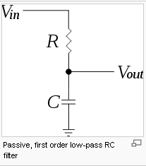
To remove the high frequency components, consider
a half power point near the max frequency that you wish to pass. The
half power point or 3db down point (.707 volts below input voltage) is
give for a low pass filter to be 2pi f = 1/RC. Let's consider the case
for smoothing a 1 KHz signal. Choosing 2 KHz for the 3 db down point
gives 6.28 × 2000Hz × RC = 1. We must choose common RC
values. Starting with 1K ohm resistor gives a C of 0.08 UF (micro
farads or 10^-6 farads). The closest value in the lab is .068 uf. This
will produce a 3db frequency of ~2.34KHz. Close enough!
Set the source signal to 1 KHz sine wave. Observe the DAC output.
Notice the quantizing steps in the output wave form. With the input and
output waveforms displayed on the scope, it should look something like
this.
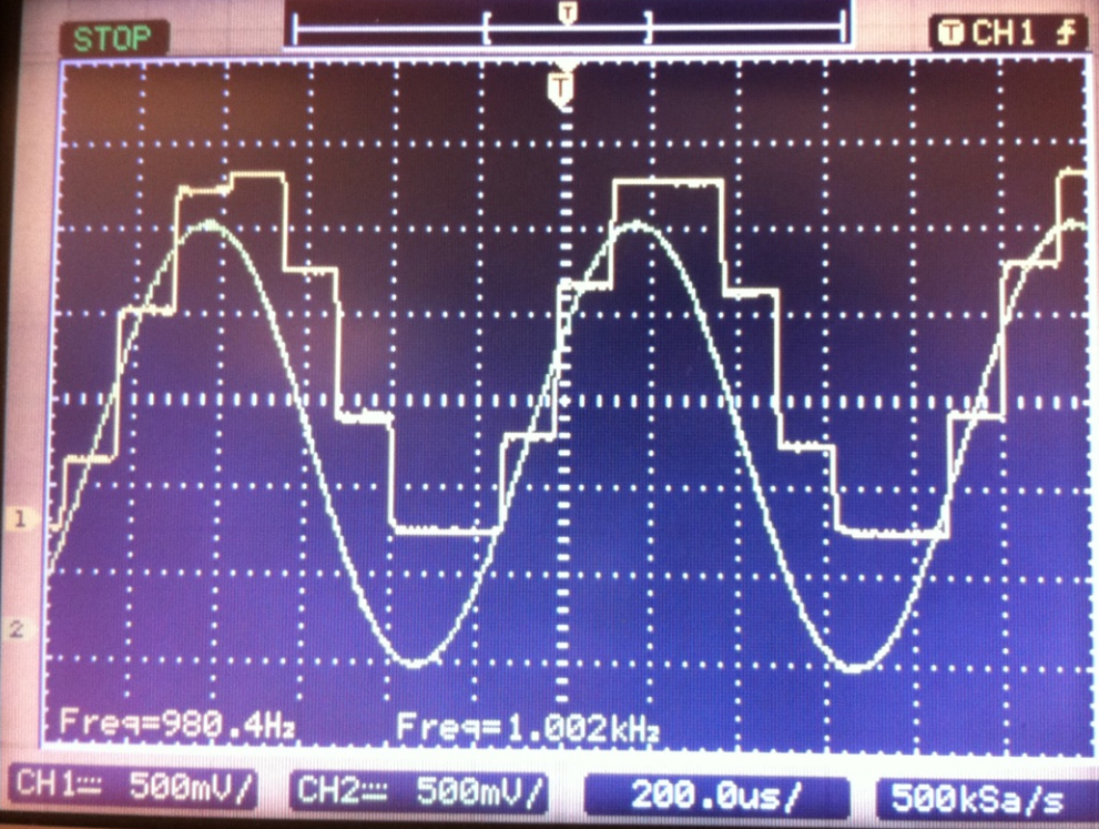
For the post lab, record the number
of quantizing steps there are per cycle.
Construct a low pass filter with a 1K ohm resistor and 0.068uf
capacitor on a protoboard. Wire the DAC to the input of the filter and
observe the output.
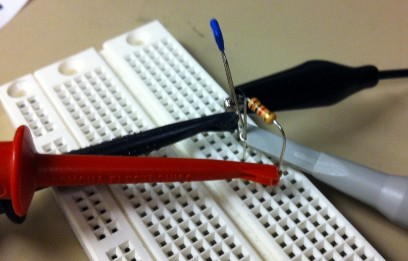
You should notice a signal that is pretty close to a continuous sine
wave. The signal will be attenuated because of the filter.
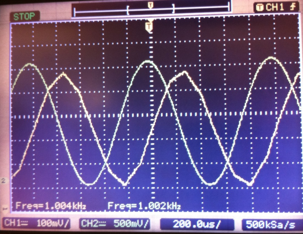
The filter output amplitude should be about 0.707 the value of the
input voltage value at the 3db down frequency (2.34KHz) . Notice that
it is considerably lower. Adjust the frequency until the filter output
value is 0.707 the value of the source frequency and record the frequency for the post lab.
Measuring Quantization Error
In order to observe the ADC result correctly, we output the data
through screen instead of
using the scope. Adding the following line in the while(1) loop. Follow
lab 5 instructions to setup UART_0 for printf output.
printf("adc_result: %u\r\n", (adc_data>>4));
You will measure the transition or boundary voltages for the first 4
ADC conversion values 0, 1, 2 and 3. The lab power supply 0-6 volts
output can be adjusted to ~ 1mv, so you can use this as a voltage
source. The voltage meter on the power supply is not accurate enough
for 1 mv measurements, so you should use the DMM. Be sure to use the
cable configurations shown in the following configuration or you will
introduce interference that will make it difficult to resolve the
transition voltages.
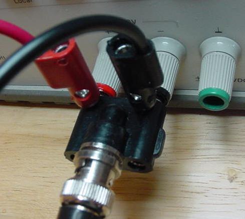
TAKE CARE TO MATCH THE GROUND TAB
ON THE BANANA PLUG TO BNC ADAPTER TO THE GND PLUG OF THE POWER SUPPLY
OR YOU WILL SMOKE THE SMARTFUSION KIT!
The procedure for measuring the transitions voltages is to simply
start at 0 volts then gradually increase the voltage until you see the
conversion value change. The voltage at which the ADC conversion value
changes Is the transition voltage. You will find that the
transition voltage does not occur neatly on distinct boundaries. In
fact, it
will toggle between adjacent conversion values for several millivolts.
It will look something like this
Input Voltage (mv)
0-------4-------8--------------14-------18--------------24-------28--------------etc
Conversion Value
0,0,0,0-1,0-1,-1,1,1,1,1,1,1-2,1-2,1-2,2,2,2,2,2,2-3,2-3,2-3,3,3,3,3,3,
The conversion
uncertainty over the transition boundary is from signal variation
in the source voltage. In other words, it is an error source from the
measurement procedure. It is NOT from ADC quantizing. You can
assume the first voltage reading that is associated with an unstable
conversion value is the transistion volage for that interval. For
example, in the above example 0 to 4mv is the conversion interval for
0, 4mv to 14mv is the conversion interval for a value of 1, etc.
Mearsure the
conversion value as a function of the input voltage as shown above for
conversion values 0 through 3. Save these values for your post lab
report.
| Voltage
Range (mv) |
Conversion
Value |
|
0
<---> |
0 |
|
<---> |
0<-->1
unstable |
|
<---> |
1 |
|
<---> |
1<-->2
unstable |
|
<---> |
2 |
|
<---> |
2<-->3
unstable |
|
<---> |
3 |
|
<---> |
3<-->4
unstable |
Reading Accelerometer Signals with ADC
For this part of the lab we will use the ACE, ADC to acquire the
signals of a typical device: the Freescale
MMA7361L triple axis accelerometer. This sensor is commonly
used in EECS 373 projects and represents a typical analog device
interfacing application.
Breadboard the Accel
When testing or characterizing devices, it is convenient to use a
prototype board (protoboard) or breadboard. The board we will use is
the Sparkfun Breadboard.
For more information about protoboards see Wikipedia : BreadBoard.
In this case, we will provide power, control and output signal
connections between the protoboard and SmartFusion expansion card.
From the specification you will see the accelerometer is a surface
mount device. To make connections to this device, you will have to
solder little wires onto the pads or better yet use what is known as a
breakout pcb to facilitate the connections. You may have to do
something like this if you use such a component in your project.
Fortunately, Spark fun provides this component mounted to a PCB board
with convenient solder points connected to the device pins.
Here is the link Sparkfun
MMA7361L Kit . We have even soldered on a set of pins (a
header) so you can plug it into the protoboard.
The first order of business when breadboarding a device is to determine
the power connections and requirements. You will find in the
specification that the accelerometer requires 3.3 volts. It is
important not to exceed the maximum rating or apply the voltage in
reverse (negative voltage) or you will smoke the device.
Place the accelerometer in the protoboard as shown below. You may
have to rock the pins a bit to get it to go in the protoboard.
The power pins are labeled GND and VCC on the accelerometer
board. Rather then hook the power directly to these pins, jumper them
over to the power rails on the protoboard. Supply 3.3 volts to the
power rail from the expansion board or you can use a power supply. If
you use a power supply, use the banana plug terminals on the protoboard
to make the connection. You will also need to provide a GND connection
from the expansion board or power supply.
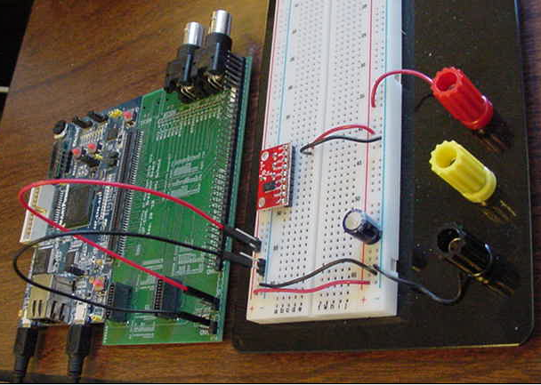
Notice that a decoupling capacitor is added across the power
rail. This is generally good practice when using a protoboard. Notice
also that a header pins are used to make some of the connections. These
are very handy when working with protoboards. They are available
in the lab in 40 pin lengths and can simply be broken to shorter
lengths as shown in the protoboard.
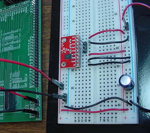
Next it is necessary to provide inputs to a few of the control signals
on the accelerometer. There is a self test control input labeled
ST and a gain select labeled GSEL that will need to be set to
GND. There is also a sleep mode that must be disabled by applying
VCC to the input. This pin is labeled SPL. The 0GD pin is an output
that will signal when 0 G is detected. In addition you should add some
header pins to the X, Y and Z outputs so you can easily attach a probe
or jumper. Additionally, put a jumper in the GND rail to conveniently
attach your scope probes.
Observing the Accelerometer Output with the Oscilloscope
When using devices for the first time, it is helpful to get a sense for
their performance by observing the behavior with standard lab
equipment. Lets try this with accelerometer by observing its behavior
with the oscilloscope. The accelerometers gain is set such that
the accelerometer will detect +/- 1.5 g maximum. You can use gravity as
your yardstick. Connect a scope probe ( a real scope probe, not grabber
clips) to the Y axis output. Make the following measurements. Save your
values for your post lab report.
When the protoboard is oriented flat on the desk, what value do you
read?
When you tilt the board to the right, what smallest value do you read?
When you tilt the board to the left , what largest value do you read?
Voltage Scaling and Buffering
Scaling
The accelerometer will potentially produce a full scale voltage near
its supply voltage or 3.3 volts. You can observe this on the
Oscope by shaking the sensor exceeding +/- 1G. This can be a problem if
you want to observe sensor extremes on the ADC. The ADC can not measure
voltages exceeding its reference voltage of 2.56 volts. Voltages
exceeding 2.56 volts will be capped. If you want to measure
forces at this extreme you will have to scale the accelerometers
voltage
range of 0 - 3.3 volts to the ADC range of 0 - 2.56 volts.
In this case we need to reduce the signal by the scaler 2.56 volts /
3.3 volts =
0.7758. Since we are reducing the signal, it is possible to reduce the
voltage with a simple voltage divider.
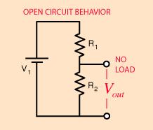
Where Vout is equal to Vin (R2 + (R1 + R2)). See this link
for more details. Using standard resistor values it is possible
to achieve the correct scaling with R1 = 2.7K and R2 = 10K. This will
result in a scaling multiplier of 0.7874. Close enough!!
Loading From Source Voltage
You will find that if you connect this circuit to the
accelerometer it will not scale as expected. This is because the
accelerometer output does not act like an ideal voltage source (no
source resistance). There is an output resistance that is in series
with the voltage source that will combine with R1 to change the voltage
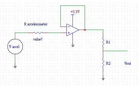
divider ratio. The circuit is modeled like this.
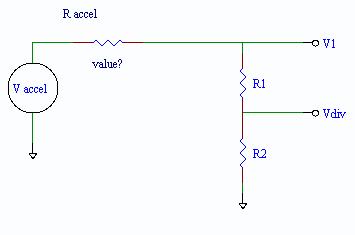
Determine R accel.
Hint: Vaccel is can be determined by measuring the
open circuit voltage at V1 (R1 and R2 disconnected). Then measure V1
under the load of R1 and R2. Be sure to keep the
accelerometer stable during these measurements.
Provide your calculations and findings for the answer sheet in the Post Lab.
You can isolate the accelerometer from the divider
with a impedance buffer or more commonly known as a voltage follower.
The voltage follower has a very large input resistance and a very
small output resistance. As a consequence, it does not load the source
voltage and does not load the voltage divider. The voltage follower can
be implemented with an op amp as follows.
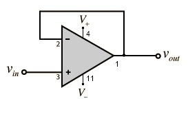
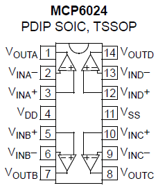
A very handy op amp for this purpose is the Microchip MCP6024
. It has 4 op amps in the same package and works well for our
voltage ranges. The following showes how to connect the buffer and
divider.
On your protoboard, wire the scaling circuits for all 3 accelerometer
axis using the op amp buffer. You can
supply the op amp chip with 3.3 volts from the expansion board. You can
check the output of the divider for correct scaling by using the
Oscope. Do not connect to the ADC yet.
Loading From the ADC Input Channel
The input resistance of the ADC can also act to load R2 of the
voltage divider. It manifests as a resistor in parallel with R2.
Therefore, if the load resistor is large, the effective parallel
combination of R2 and the load resistor will be R2 or it will not
effect the voltage divider. Fortunately, this is the case with our ADC
and there is not need to buffer or compensate the divider for loading
effects.
Note, before you can attach the
divider to the ADC input channels, you will have to program the ACE to
enable these channels (below) or you may observe loading effects.
Providing more ADC channels
You will have to add 2 more ADC channels for the post lab assignment.
To do this follow the procedure above adding 2 more ADC Direct
Input services in the ACE. You can provide any service name you
like, but the pin numbers must be specific to the kit. The following
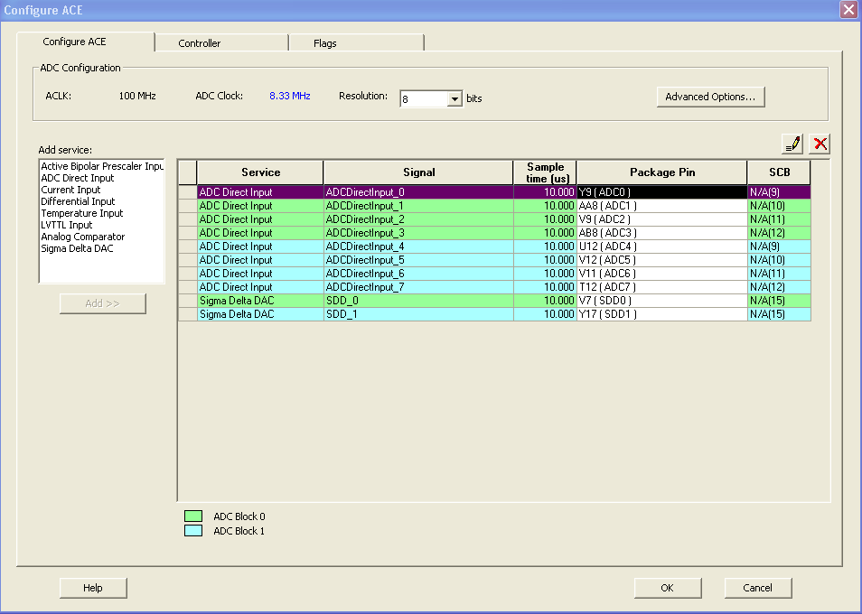
screen shot shows all the possible ADC and DAC channels configured. The
service names are chosen to reflect the respective ADC channel. Note,
although ADC0 and ADC1 are shown in this configuration for
completeness, they are not connected to the SmartFusion kit with this
version of the expansion board. ADC2 through ADC7 are available.
Configure the ACE ADC for 3 inputs or services.
Remember to Generate in the MSS. This will add the additional hardware
and update the ADC drivers. You will have to copy the updated drivers
to your softconsole project.
The ADC channels are referenced in the ADC drivers with the Signal
names choosen in the ACE, ADC setup. For example, to add ADC channels 2
and 3 consider the following code.
#include <stdio.h>
#include <inttypes.h>
#include "drivers/mss_ace/mss_ace.h"
#include "drivers/mss_uart/mss_uart.h"

ace_channel_handle_t adc_handler2;
ace_channel_handle_t adc_handler3;

int main(){
    ACE_init();
    /* DAC initialization removed */

    adc_handler2 = ACE_get_channel_handle((const uint8_t *)"ADCDirectInput_2");
    adc_handler3 = ACE_get_channel_handle((const uint8_t *)"ADCDirectInput_3");


    while(1){
    	uint16_t adc_data2 = ACE_get_ppe_sample(adc_handler2);
	uint16_t adc_data3 = ACE_get_ppe_sample(adc_handler2);
    }
    return 0;
}
Post-Lab Assignment
Write an application program so that the LEDs mirror the accelerometer status.
That is, when the board is sitting flat the middle LEDs should be illuminated,
as the board is tilted, the LEDs should reflect the current board position:
LEDs:   00011000      10000000      0000001

                           /          \
BOARD:  --------          /            \
                         /              \
                        /                \
Selection through the 3 accelerometer axes with the push buttons. You can choose
the switch combinations and it is OK if you have to hold the switch to maintain
the selection. Consider using the builtin MSS GPIO module to provide your LED
and switch hardware interface (this will involved opening the MSS configurator,
configuring the GPIO block to route GPIOs through the "Fabric" (FPGA), and then
mapping the GPIOs to the LEDs and switches).
Post-Lab Questions
The post lab questions can be found on this answer sheet. Use this form
to submit your answers or copy into to a word processing program.