
Copyright © 2010-2011,
Thomas Schmid,
Matt Smith,
Ye-Sheng Kuo,
Lohit Yerva,
and Prabal Dutta.
10/26/2011
The purpose of this lab:
Assume you are given the following application by a customer who is unhappy about the application performance. The application connects to the serial port of your computer through a serial console (e.g. putty or Hyper Terminal), and outputs information on the OLED display of the SmartFusion evaluation board. The application reads commands from the serial port, and changes the output on the OLED display accordingly.
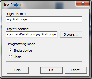
Program your SmartFusion with the following FPGA programming file oledFpga.zip. You won't need to run Libero for this. Unzip the file and launch FlashPro directly from the Start menu (You can use Start->run then type flashpro and hit OK). Click on the New Project button

Change the project location to a convenient folder, e.g. the folder
to where you
just unzipped the FPGA programming files. Then give the project a name,
e.g.
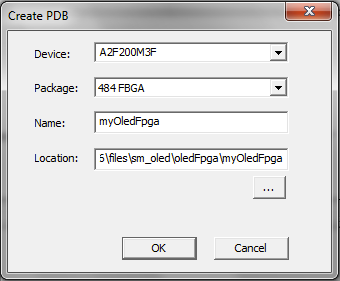
We now have to configure the programming file. Click the Configure Device button. You will get some new optional buttons. Click the Create... button just below Browse....

Configure the next dialog for the A2F200M3F in a 484FBGA package.
On the next dialog, we have to configure the FPGA Array and the Embedded Flash Memory. Click the check box next to the two settings and select the corresponding files in your unzipped folder.
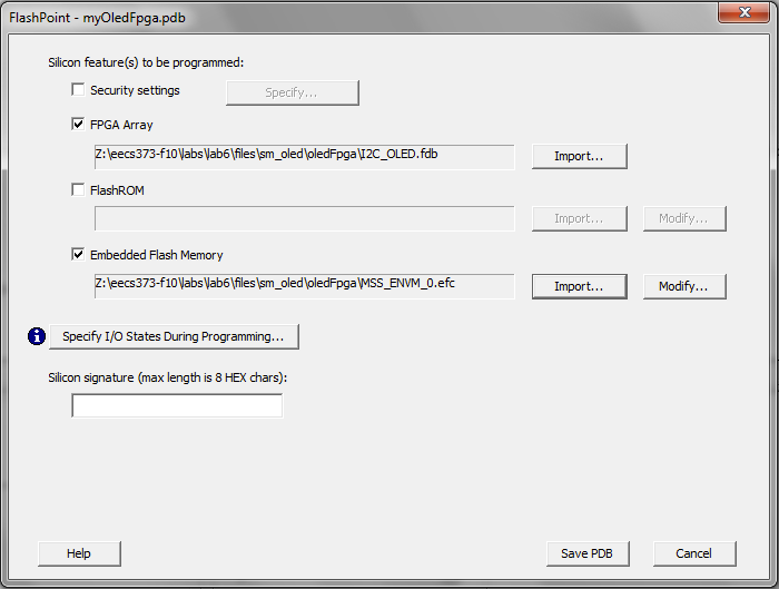
Once the files are imported, click the Save PDB button. We are now ready to program the SmartFusion. Go ahead and click the Program button.
Download and unzip the following SoftConsole workspace oledSoftware.zip. Note, this is a SoftConsole workspace. Thus you have to use the File->Switch Workspace->Other... menu option in SoftConsole in order to open it up.
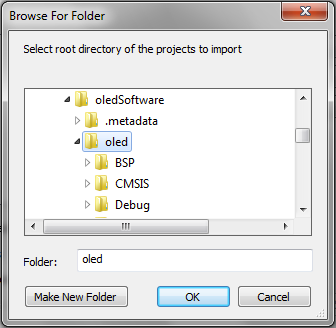
In the Workspace Launcher window, click on Browse... and find and select the unzipped folder that contains the .metadata folder (but not the .metadata folder itself).
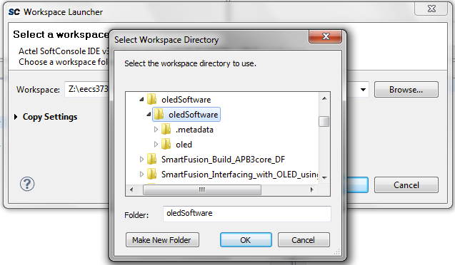
Once found, click OK. SoftConsole will close, and relaunch using the new workspace. The workspace is configured with one project called oled.
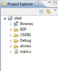
If the project doesn't appear, then just import it by right-clicking into the Project Explorer then select Import.... Choose the option General->Existing Projects into Workspace. On the next screen, click on Browse... to select the root directory of the oled project and then confirm with OK, then click on Finish.
The project should now appear in your Project Explorer.
Clean and compile the project. Then, run the debugger and resume the application. You should see text appearing on the OLED display. Connect a serial terminal, e.g. Hyperterm or putty. Once the terminal is connected, hit the key 5 on your keyboard. You should see a sine wave appear on the OLED. After a while, some text gets output on the serial console. This is the option menu. Try out some of the different options (1, 2, 3, 4, or 5) and notice how the OLED changes its behavior.
You will quickly notice that the application blocks until a display
mode is
finished, before it switches to the next display mode. Stop your
debugging
session and return to the main function of the
application.
How does the application initialize the UART connection? What is the
UART
speed and configuration? How is this different from earlier uses when
you
output data using printf?
Find the infinit while(1) loop and notice how it uses a
blocking
polled read from the UART using the readchar() function
defined
in main.c higher up. This function blocks, until it
receives a
character from the UART. Once received, a large switch
block
changes the output on the OLED display. The problem with this program
flow is
that you always have to wait until the OLED procedure is done. There
are many
delay and busy loops inside the switch block making sure
that the
OLED has enough time to display things, before a new key can be
pressed. This
behavior is undesirable. What we would like is an immediate reaction on
key
presses.
Change the application such that it reacts immediate on key presses and
changing the output mode of the OLED accordingly. Instead of using a
polled character read function, you will have to use interrupts. Look at the
UART driver in drivers/mms_uart, especially the
MSS_UART_set_rx_handler() function definition in mss_uart.h,
to find out how to subscribe to interrupt events,
and configure the driver for interrupt driven
communication. In addition, you will have to change the switch
block for the new behavior. Consider how you can use a global variable
that is set in the UART interrupt service routine to exit loops and delays
in the switch block. For instances, much time is
spent in the delay function. This would be a good place to use
the global variable to exit the delay loop. Note that you don't
have to check for a change of state after every operation.
Human reaction time is around 100 ms. Thus, if you
react to a key press within that time, we can't really differentiate if
it was immediate or not. Last thing to note: If a case statement cannot
finish (by braking at the middle) some of the OLED setting might not get
reset for another case statement's proper display.
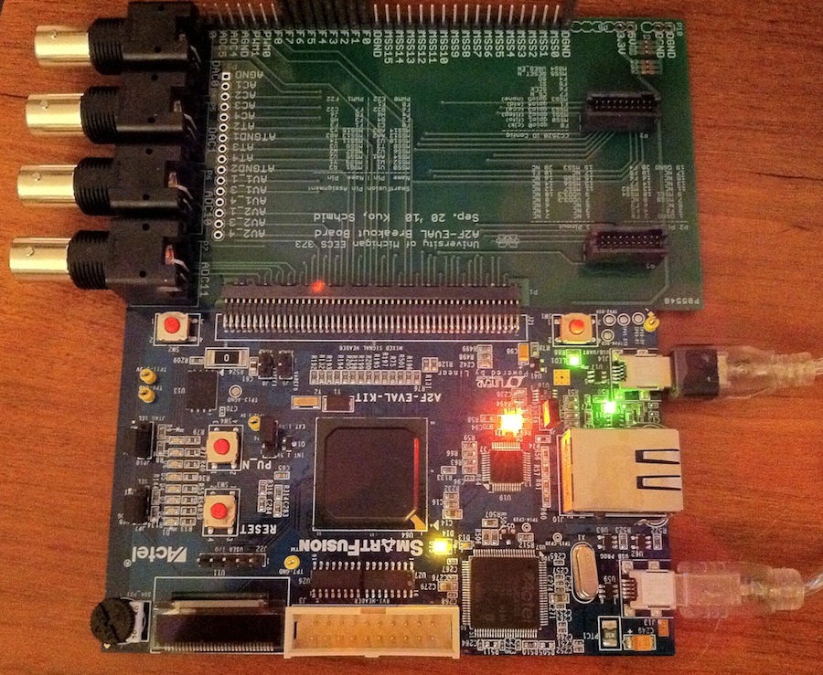
A project breakout board will be provided for you that makes connections to the header pin on your SmartFusion kit mechanically easier. It also has a radio kit installed for communications between SmartFusion kits. Interfacing to the radio is accomplished over a serial bus interface SPI. The Saleae Logic Analyzer has the ability to observe serial bus transmissions in simple digital or decoded form. We will use the logic analyzer to observe transmission between the SmartFusion kit and radio.
In this exercise, you will learn how to use the logic analyzer to
decode serial protocols. First, program your FPGA with the following
Libero
project serialAnalyzerFpga.zip.
Don't worry if you see some Error: Core ... errors. Just program the board
using FlashPro.
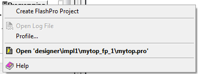
Note, if opening the programming file in FlashPro fails, then click on
the
small downward arrow on the Programming icon in your Project
Flow and select Create FlashPro Project. This will
regenerate
the programming file based on your new file structure.
Once the FPGA is programmed, download and unzip the following
SoftConsole workspace serialAnalyzerWorkspace.zip.
As before, switch the workspace using
This workspace is a little special. It contains a pre-compiled binary,
and the
main.c file got removed. While you can still launch the
debugging
session, you won't be able to look at the code itself. Therefore, you
will
have to use an external tool, the logic analyzer, to find out what the
application
is doing, and how it is configured.
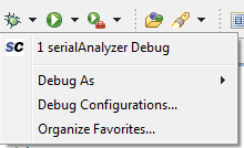
Launch the debugging session
This will start the debugging session and upload the binary to the
SRAM. Once
done, the debugger will stop. However, you won't see any code as you
are used
to. This is because we removed the debugging flag from the compiler.
Just
resume  the session, so that the
application can continue to run.
the session, so that the
application can continue to run.
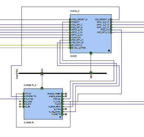
As you might have seen from the Canvas in Libero, the application uses three core peripherals to communicate with the outside. We instantiated a CoreSPI, CoreI2C, and CoreUARTapb. The application configured each of these cores in a certain way. Your job is now to find out what the individual serial configuration of each core is by answering the questions below. To facilitate your task, you can use the Saleae USB Logic Analyzer.
First, unplug your A2F Eval board from the USB cables and make sure you assembled your new A2F breakout board. Then, connect the breakout board to your A2F evaluation board. The two boards should snap together tightly.
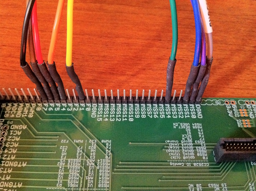
Connect the Saleae USB Logic Analyzer to your computer. Next, connect the 9 wires to your breakout board as shown on the picture. Note, the gray wire is ground and should be connected to DGND. The next wire, violet, is connected to F0. All the other colors follow in order from that point on.
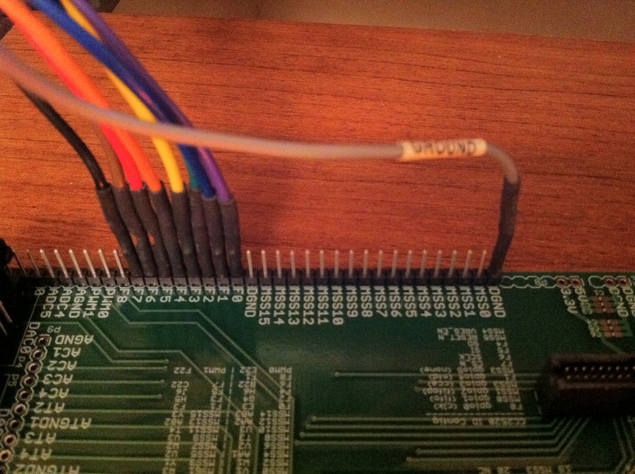
Then, connect the other side of the 9 wires into the logic analyzer pod. Make sure that the gray wire is connected on the side which shows a ground symbol, and the black wire near the "1" sign.
You are now ready to start the Saleae Logic application on your
computer. You
should be able to find it in your Start Menu under
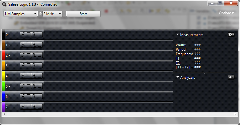
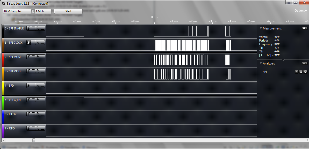
Make sure the title of this window says [Connected]. This means that the application found the logic analyzer hardware. Then, make sure your application is running on your smart fusion MSS. Set the sampling buffer to 1 M Samples at 2 MHz as shown on the screenshot above. Then hit Start.
The screen should have filled with some data. Use the mouse to zoom in (scroll wheel). The following table will allow you to identify what each color means.
Identify the peripheral to which each signal belongs. Hint: Take a look at the top level canvas in Libero to trace the signals to the respective devices.
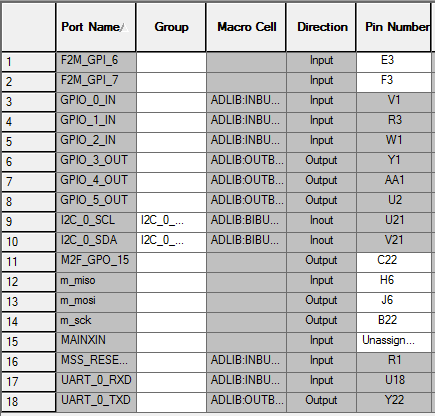
| Signal Name | Pin Number | Breakout Name | Peripheral Name |
|---|---|---|---|
| MISO | E3 | F0 | |
| MOSI | F3 | F1 | |
| SCK | G4 | F2 | |
| CS | H5 | F3 | |
| RX | H6 | F4 | |
| TX | J6 | F5 | |
| SDA | B22 | F6 | |
| SCL | C22 | F7 |
Next, let's add some serial analyzers. The serial analyzers decode for
you
the logic levels into human readable values. On the right hand side of
the
Logic application, click on the "+" button near the text  . On the drop down menu, select
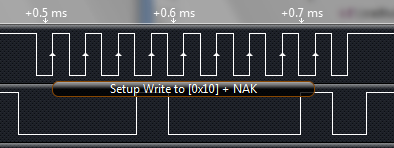
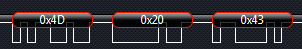
On the next screen, you have to configure your I2C decoder. First, you have to select the two wires for I2C, SDA and SCL.
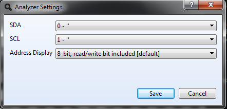
Then, click
If you selected the right two wires for the I2C Analyzer, then you should now see the decoded values of the I2C protocol. If you zoom in even further, the Analyzer shows you start and stop conditions too.
Similar to the I2C analyzer, add an analyzer for SPI, and another one for Async Serial. Note, you will first have to analyze and identify the different signals in order to configure the analyzer correctly. Once you figured out the configurations, the analyzers will show you the different data bytes decoded.
Using the different logic analyzer capabilities answer the following questions for the different serial protocols. Note that the top right block shows you measurements of the signal if you move your mouse over the different bits. It might also be necessary that you sample at an even higher rate than 2 MHz. Remember, with a 2 MHz clock, you have a time resolution of 0.5 us, which is potentially not enough to find the frequency of a measured clock signal. Make sure you measure average transfer rates over a significant amount of time, not just over one transfer (e.g. 100ms to 1 second).
Hint: Take a look at the top level canvas in Libero to
trace the signals to the respective devices.
The UART uses 8 bit data. Answer the following questions using the logic analyzer.
Give at least two potential improvements in order to speed up transfer on all the serial protocols.
In this last part of the lab, you will learn how to write a peripheral driver. In this particular case, you will write a driver for the CoreSPI component to allow a radio driver to talk to a Texas Instruments CC2520 radio.
Often times in embedded systems, you will have a driver for an external component, such as a radio, that is written in a hardware independent way. It is the job of the serial peripheral driver to provide an interface to the component driver such that it can communicate with it. The interface between the radio driver and the serial driver is often called a Hardware Abstraction Layer (HAL). Embedded operating systems often times provide a rigorous set of HAL specifications such that they can easily be ported to new platforms.
The following file contains the Libero project for this exercise cc2520Fpga.zip. Open it up and look at the canvas view of the wiring diagram. You can see that we instantiated the MSS with several GPIO inputs and outputs, and two peripherals, UART_0 and I2C_0. The IOs are used to talk to the radio, while the UART_0 is used for output to the serial port, and the I2C_0 to talk to the OLED display. Additionally, we instantiated a CoreSPI core on the APB3 bus with base address 0x40050000.
The pin configuration should already be saved in the project.
However, check
to make sure that it didn't get lost by comparing it to the following
picture.
Note, the
Program your FPGA with this project by synthesizing, place & route, and flashing the Smart Fusion.
To write the CoreSPI driver in SoftConsole, you will need two pieces of information
You can download the CoreSPI documentation here: CoreSPI Handbook. This document includes detailed documentation of the CoreSPI component instantiated in the FPGA. Note that we won't use the interrupt capabilities of the CoreSPI core. We will used a polled read and write.
Download the following SoftConsole workspace cc2520Workspace.zip. Open it up in SoftConsole as before by switching the workspace to this directory. If the projects are not in the project explorer, then import them as described earlier in this lab. The workspace should now have two projects defined, spiDriver and lab6cc2520. spiDriver is a very minimalistic test application which you can use to develop your SPI driver (more to this later), while lab6cc2520 is the final intended target that implements the radio driver and a small application that sends and receives messages from other radios.
It is much easier to develop a peripheral driver in isolation without having to worry about the radio or any other system components. The spiDriver project allows you just that. Open up the project in SoftConsole and look at the drivers directory. You can find a skeleton for the CoreSPI driver, including the required HAL definition for the radio in spi.h. The function definition also give you a hint of what you will have to implement. Note that we won't use the chip (Slave) select capabilities of the CoreSPI core module, as the radio driver needs special control over it. Therefore, we moved the chip select to the MSS GPIO 15 output line.
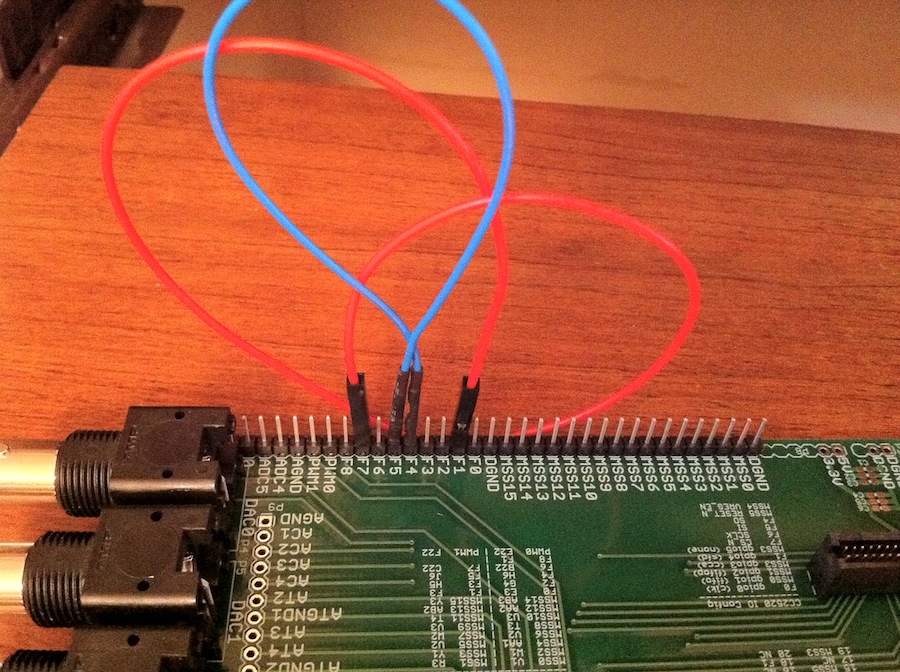
The main function implements a small functional test of
your driver. It requires you to configure two loopbacks. The first one is to
send all the data coming from the CoreSPI right back to it (MOSI->MISO
loopback, F4->F5 on the breakout board), and the second one connects
the chip select line to GPIO7 of the MSS (F7->F1 on the breakout board). The bin containing
expansion boards and Radios should contain a bag of wires. Find the correct type (female to female). The
following picture illustrates this:
I highly suggest that you choose the slowest clock possible for SCK when you intialize the SPI peripheral in the next exercise code. There are two reasons for this choice. First, in case you want to connect the logic analyzer to it, the slower the clock, the better it can handle it. Second, the radio driver currently has issues with fast SPI clocks. While the Radio can handle SPI clocks up to 8MHz, the driver has some concurrency issues. Thus, for now, choose the biggest clock divider configurable on the CoreSPI.
You can also get creative and connect, together with the loopback, the logic analyzer and visualize your SPI communication. However, it will necessitate you to breakout the signals to a breadboard. Breadboards are available in the 373 lab.
Implement in drivers/CoreSPI/core_spi.c the functions
defined in
drivers/CoreSPI/spi.h by using the register definitions
and
functional descriptions from CoreSPI
Handbook. You will have
to read the handbook to find out how the CoreSPI verilog peripheral
works, and
which registers perform what operation. Note that your driver will not
have to
worry about any sorts of interrupts. However, you will have to
busy-loop on
certain status register bits in order to make sure that a byte transfer
has
been finished, before you return. Test out your driver by running
compiling
and running the spiDriver application on your SmartFusion Eval
board.
Check the serial output using Hyperterminal or Putty to see if the
small
checks implemented in the main function
succeeded or not.
Once you are convinced that your CoreSPI driver works, copy the driver over to the lab6cc2520 project. Then, compile your code using the special Debug Radio configuration. This configuration adds code optimization to the compile stage. Without optimization, the application would be too big to fit into the 56k of SRAM available. To do the modifications to the build target manually, right click on the lab6cc2520 project and select Properties. Under C/C++ Build->Settings->GNU C Compiler->Optimization you can change the Optimization Level to -O1. In addition, add to Other optimization flags an optimization for size -Os. This will instruct the compiler to remove dead code. However, as you will notice if you try to debug the radio code, debugging becomes much harder as the execution flow, due to optimizations, might not correspond to your C code anymore.

If the compilation works, program the MSS with the newly created binary. If everything works, then the OLED should show you the messages that it received (d: destination address, s: source address, c: counter value). You can also connect a serial terminal to your board. The serial output will provide you more details on what is received, and when your board transmits a message.
For debugging purposes, you can also connect the logic analyzer to observe the messages going to and coming from the radio. Use the following connection hookup
You can also load the following configuration for your logic analyzer CC2520logicsettings.zip. This will give you a configured SPI analyzer as well as the names of some more interesting signals coming from, and going to the radio.
The radio driver is fairly complex and it would be out of the scope of
this
particular lab to explain its inner working. However, its public
interface is
fairly simple to understand. All the public functions are defined in
cc2520driver.h. By including this header file, you get all
the
access to the radio for initializing the radio, turning it on and off,
putting
it into standby, changing the radio channel, and sending and receiving
messages. The header file has some more explanations of the different
function
calls, and what their parameters mean.
The steps to use the radio are as follows:
Radio_init()RadioState_turnOn()Radio_receive(...)
gets called.Radio_send.
The function Radio_sendDone will get called once the send
is done. This indicates you can send the next message.During Radio_init() several different things happen.
First, all
the I/O lines get configured and setup. Second, the voltage regulator
VREG_EN gets pulled high. The driver then starts a timer to wait
for
the radio to power up. Once the timer expires, the default
configuration is
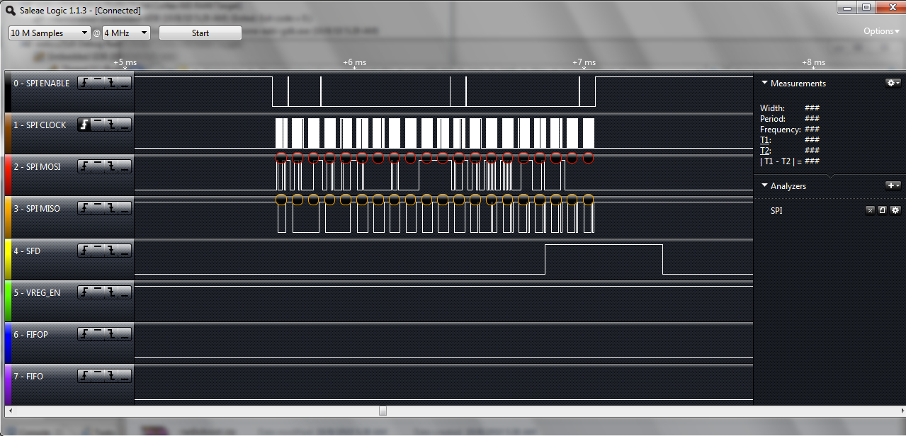
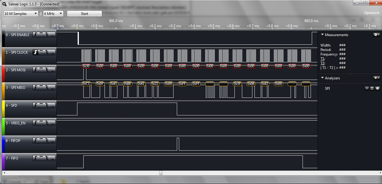
sent to the radio. The following figure shows the logic analyzer
recording the
bootup sequence.
You can load this configuration, including the recorded data, into your logic analyzer application using the following file: radioboot.zip. This allows you to zoom into the data trace and see the actual bytes sent to the radio.
Upon transmission of a message, the driver sends configuration plus the
message data over the SPI bus to the radio. After uploading the header
information, the driver instructs the radio to start sending out the
message,
while continuing to upload the rest of the message. The Start of
Frame Delimiter signal (SFD) gets pulled high by the radio,
indicating that a transmission is starting. At the end of the
transmission,
the SFD line gets pulled low, indicating to the MCU that the
radio is
ready to send the next message. At this point, the driver calls
Radio_sendDone(). The following is the execution trace as
seen by
the logic analyzer. You can use the following file to look at the data
in
detail in your logic analyzer application radiorxtx.zip.
When the radio receives a message from another node, it pulls up the SFD line. This indicates to the MCU that it can start downloading the message from the receive FIFO. The two signals FIFO and FIFOP are used by the MCU to find out the state of the receive buffer. The following image shows the connections as seen by the logic analyzer. You can use the following file to look at it in more details: radiorxtx.zip
We use a C structure to create a payload for our message. To assure
that our
message is nicely packed into memory, we use the
__attribute__((__packed__)) modifier. Look at the
blinkmsg_t definition in main.c for an
example.
There is one more thing one has to take care of if one communicates
with
another system. It could be that the byte order of the two systems is
different. Thus, by convention, one usually communicates in network
byte
order, or big endian. Since our system is little endian, we have to
translate
all the data we send over the network from little endian to big endian.
You do
not have to do this for the parameters you give to Radio_send
as
the radio driver takes care of them. Only the payload, which is under
your
control, has to have its data types in big endian. To translate from
little
endian to big endian, and vice-versa, you can use the functions defined
in the
htons.h file. Note: hton stands for
host-to-network, and
thus translates from little to big endian, while ntoh reverses
this.
Finish your CoreSPI driver and get it to work with the radio.
You may work with a partner for this assignment.
During the next lab, show that your radio transmits messages. We will
have a
receiver station connected to one of the stations which will log all
the
source addresses. In order to not have the same source address as
another
group, choose a random uint16_t number and set it in your
main.c as the SRC_ADDRESS define. This will
allow
you to identify and differentiate your messages from other groups.