
Copyright © 2010-2011,
Matt Smith,
Thomas Schmid,
Ye-Sheng Kuo,
Lohit Yerva,
and Prabal Dutta.
08/28/2011
See posted lab schedule for due dates, in-lab, and post-lab due dates.
In this lab you will learn to:
This lab document is quite lengthy because of the many screen shots and detailed procedures. This is a necessary introductory phase to get you acquainted with the various tools. While the document is long, you should be able to finish the In-lab section within the lab period. You may also get a good start on the Post Lab assignment, but will likely have to finish outside the lab period. You will be given 24 hours access to the lab the first lab period via keypad entry so that you may use the lab at your convenience. There will also be additional supported open hours that will be posted on the course webpage.
There is no Pre-Lab assignment for this lab. The lab requires no preparation; however, consider:
Implementing Simple Hardware for the SmartFusion FPGA
Observing Logic Function with the Oscilloscope
Measuring Propagation Delay with the DSO
Observing Logic Function with the Logic Analyzer
Measuring Power Consumption with the Multimeter
The Libero IDE Project Manager organizes the SmartFusion hardware development tool chain with an intuitive GUI. Libero is installed on the 373 workstations. Libero is also available free from Actel with all the functionality required for the course. Libero is not currently available on CAEN loads.
Begin by opening the Libero Project Manger. ![]() Libero will open with the following view.
Libero will open with the following view.
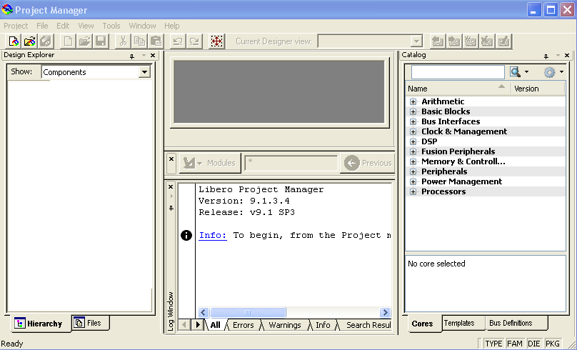
The left most window is the Design Explorer and will show all the design modules and files associated with your project. The top center window will show the tool chain design flow and selected design files. It is not populated until a project is opened. The lower center pain reveals the output from the various commands evoked from the GUI. The left most pain contains a library of various prebuilt logical functions from simple logic gates to entire processors!
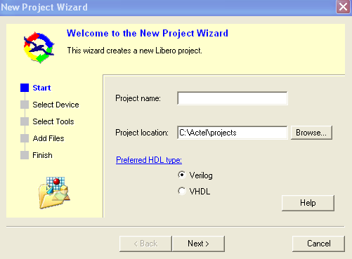
Open a new project by selecting Project![]() New
Project from the drop down menu.
The following screen will appear
New
Project from the drop down menu.
The following screen will appear
In this step you will specify the project location and name. You should browse to your class directory space. Enter a project name: lab1. Notice that the project name will be automatically appended to the project location path to form a new directory. Make sure Verilog is selected for the preferred HDL type. The screen should look something like the following.
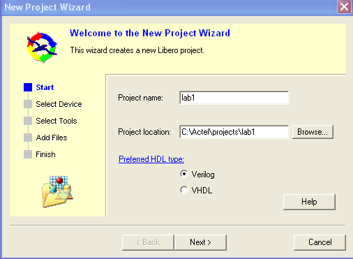
Click next and the following screen should appear.
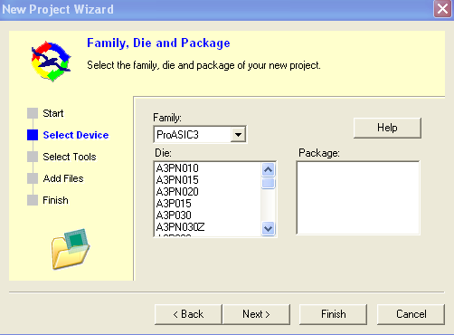
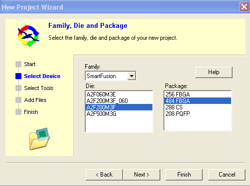
Next we need to specify the device type. Notice that the tool supports many different Actel devices. Select the following:
Click next and the following screen will appear.
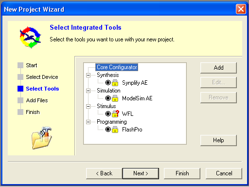
In this step integrated tools for synthesis, simulation and flash programming are selected. These were pre-set on the lab workstations. However, you will have to set these yourselves if you install software on your own machine. Follow the instructions from one of the tutorials from Actel like http://www.actel.com/documents/SmartFusion_LiberoSoftConsole_POTlevel_tutorial_UG.pdf
Click next and the following screen will appear.
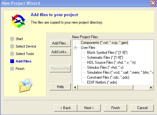
In this step additional project files may be added such as design files, simulations, etc, developed with other tools. There are no files to add so click next and the following screen will appear.
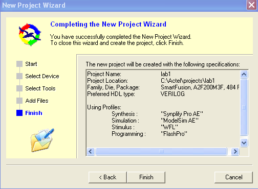
You will see a summary of the project details previously selected. Select finish and the following screen will appear.
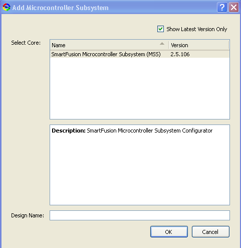
In this step the project manager is asking if you want to add a microcontroller subsystem (MSS). This consists of various cores (FPGA hardware) that will support standard peripherals of the integrated ARM processor such as timers, memory, etc. We will not use this now so select cancel. The following screen will appear.
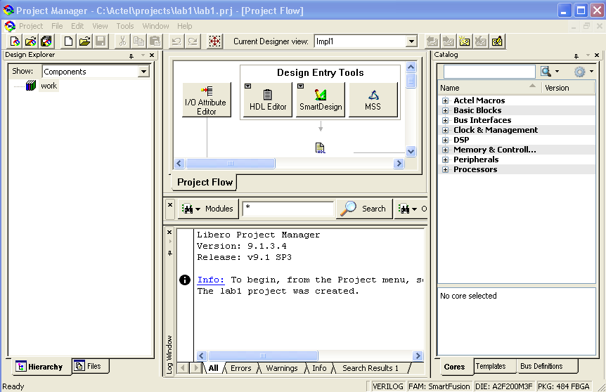
The top center pain now contains a project flow view. This shows all the tools in hierarchy and their status. The respective tool will be highlighted once the various stages of the design process are completed. Additionally, you will see the Design Explorer populated with files and components as each stage is completed.
There are several ways to specify your FGPA hardware design: block schematic, Verilog or VHDL, SmartDesign and the MSS. The block schematic and HDL methods are similar to those you probably used in an introductory digital design lab allowing for traditional schematic logic symbol entry or HDL text entry. SmartDesign is a high level functional block diagram entry method that allows for quick design entry from simple logic gates to processors. The MSS (microprocessor subsystem) method provides a graphical means to configure components such as memory, timers and interrupt controllers with the integrated Cortex M3 processor.
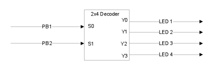
For this lab we will start with a simple 2x4 decoder entered in Verilog. The inputs of the decoder will be the two user push-button switches and the outputs will be 4 of the 8 user LEDs.
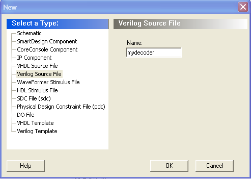
To enter the Verilog code editor click on SmartDesign, select Verilog Source File and enter mydecoder in the file name field that appears in the pop up window.
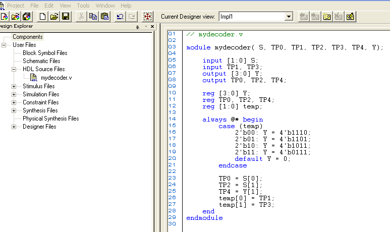
Click Ok and a new tab will open into a Verilog editor window. Copy the following 2x4 decoder Verilog code into the window and save the file.
// mydecoder.v

module mydecoder( S, TP0, TP1, TP2, TP3, TP4, Y);

    input [1:0] S;
    input TP1, TP3;
    output [3:0] Y;
    output TP0, TP2, TP4;

    reg [3:0] Y;
    reg TP0, TP2, TP4;
    reg [1:0] temp;

    always @* begin
        case (temp)
            2'b00: Y = 4'b1110;
            2'b01: Y = 4'b1101;
            2'b10: Y = 4'b1011;
            2'b11: Y = 4'b0111;
            default Y = 4'b0000;
        endcase

        TP0 = S[0];
        TP2 = S[1];
        TP4 = Y[1];
        temp[0] = TP1;
        temp[1] = TP3;
    end
endmodule
The Verilog includes porting and assignments to map some of the decoder's inputs and outputs to general purpose input/output (GPIO) pins.
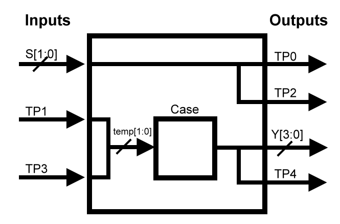
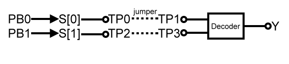
We will use these later to observe the signals with the Logic Analyzer and Oscilloscope. Notice that the switches are not directly mapped to the input of the decoder. Instead TP1 and TP3 are used as inputs to the decoder. This is necessary for observation since the kit outputs are not accessible on the kit. The test point pins will have to be connected with jumpers on the kit.
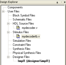
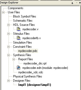
Notice mydecoder.v now resides in the HDL source files under the files tab view in Design Explorer window.
HDL syntax can be checked before synthesis by selecting the Verilog source file, right clicking and selecting check HDL file. To see how this works, remove the semicolon from the second case (01) of the case statement. Save the file and run Check Design File. In the Log window you should see the following error.
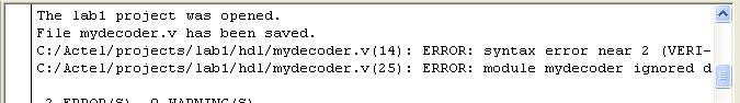
Notice a syntax error is indicated near line 14 shown in parenthesis. Correct the error, save the file and run Check Design File again. The Log window should indicate a successful check.
Try selecting the templates tab in the right window that lists the library cores. You will find templates for many Verilog and HDL constructs. For example try selecting Verilog, Common constructs, Always block, case statement. Hold the mouse pointer over case and the template for case statement appears.
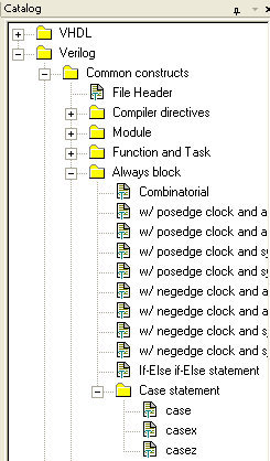
Hold the mouse pointer over case and the template for case statement appears. The template can be dragged into the HDL editor window as a starting point for design entry.
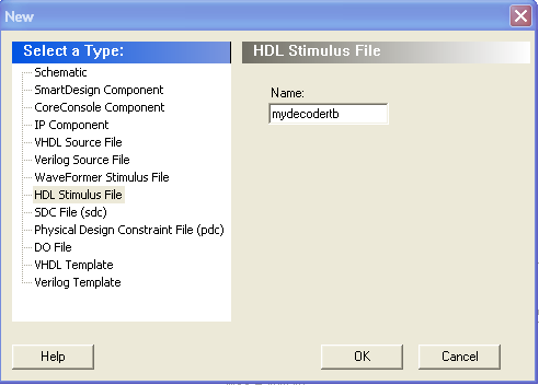
A test bench can be provided to simulate the design. Create a stimulus file by selecting SmartDesign in project flow, HDL stimulus file, enter mydecodertb in the name field.
A new window will open in the top center. Enter the following Verilog test bench.
`timescale 1 ns/1 nsNotice that TP1 and TP3 are connected to the instantiation of the mydecoder module to create the external jumper connections that will be used on the kit.
module mydecodertb();
reg [1:0]s_S; //stimulus inputs
reg s_TP1, s_TP3;//stimulus inputs
wire [3:0]s_Y; //output from stimulus
wire s_TP0,s_TP2,s_TP4; //output from stimulus
mydecoder md2(.S(s_S),.TP1(s_TP0),.TP3(s_TP2),//inputs, TP1, TP3 connected to
//TP0 and TP2 to implement external hardware connection
.Y(s_Y),.TP0(s_TP0),.TP2(s_TP2),.TP4(s_TP4)); //outputs
initial begin
//test all possible input conditions every 10ns
s_S[0] <= 0; s_S[1] <= 0;
#10 s_S[0] <= 1; s_S[1] <= 0;
#10 s_S[0] <= 0; s_S[1] <= 1;
#10 s_S[0] <= 1; s_S[1] <= 1;
end
endmodule
Save the file and now you will notice that a stimulus file has been added to the project.
Right click on the mydecodertb and do a Check HDL file to be sure the code is entered correctly.
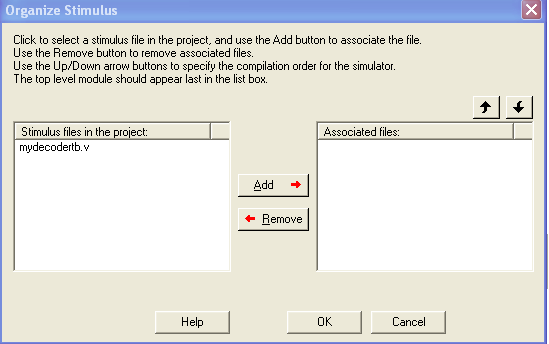
Before going any further it is necessary to tell the project manager
the
test bench module name and instantiation name. To do this select in the
menu Project![]() Setting
Setting![]() Simulation Tab and the
following window will appear.
Simulation Tab and the
following window will appear.
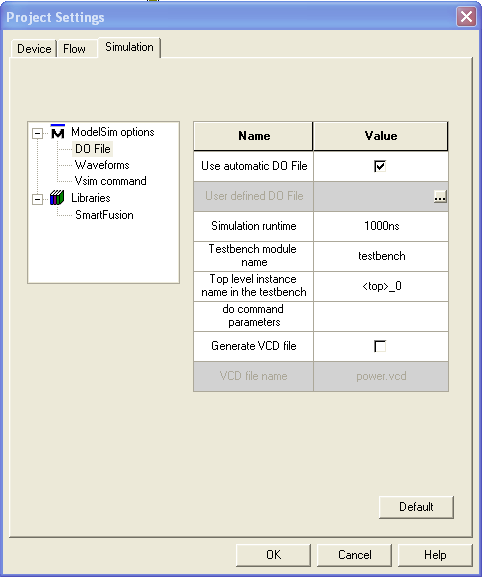
Change the testbench module name to mydecodertb and the top level
instance
name to md2 as named in the test bench. Click OK. Finally you must tell
the
project manager the name of the stimulus file. Select Project![]() File
Organization
File
Organization![]() Stimulus. Select
mydecodertb.v and ADD. Click
OK
Stimulus. Select
mydecodertb.v and ADD. Click
OK
You are now ready to synthesize your decoder. To evoke the synthesis tool, double click on the synthesis block in the project flow window. This will open the Synplify Pro synthesis tool. The following window will appear.
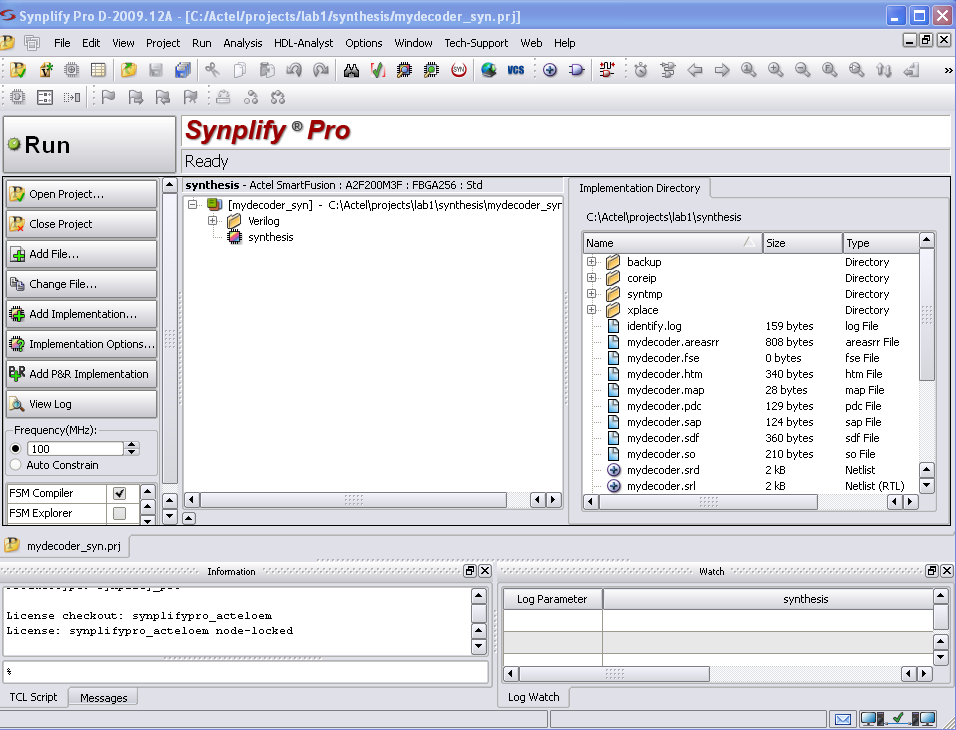
The Libero project manager has loaded all necessary project files to the synthesis tool including your design files. You can see them listed in the directory in the Synplify right window. Click the big Run button to synthesize. If the synthesis is successful you should see a message in the bottom center window of the project flow window indicating success and the Synthesis function block should turn green. Post-Synthesis files will be added to the Project Explorer Files view.
If there is an error, the block will be red. You can inspect the synthesis log in Synplicity for error specifics.
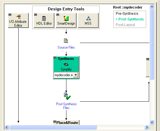
It is possible to run a functional simulation at this point or a simulation based on the decoders logical function. To model the physical implementation it is necessary to implement the decoder on the FPGA. Place and Route maps the logical function of the decoder onto the SmartFusion FPGA and provides device specific modeling information such as propagation delay to the simulator. Before running place and route, we will assign the FPGA pins that connect to the switches and LEDs.
To assign the FPGA pins connected to the switches, LEDs and GPIO we will use the IO attribute editor. Evoke the editor by clicking on the functional block in the project flow. The following window will open.
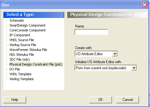
Select Physical Design Constraint File (pdc) and enter mydecoder in the Name field and click OK. The following window will open.
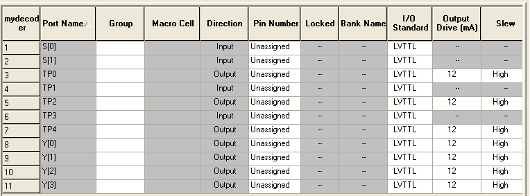
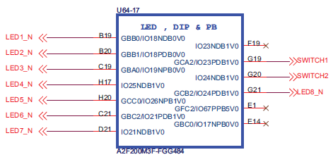
The port names and default types have been automatically imported from the top level design. The project designer does not know what pins to assign. The pins are specific to the kit and can be found in the kit reference manual. http://www.actel.com/documents/A2F_EVAL_KIT_UG.pdf. The information is provided here for convenience.
LED and Switch Pin Kit Pin Assignments
GPIO Kit Pin Assignments
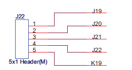
To assign the pin, click on the pin number field and scroll down to the appropriate pin number. When complete, save the file. The constraint file will now be available to the route and place tool in the project flow. You need to use the figures above to figure out which pins to use.
The file is also show in the Project Explorer file view.
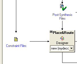
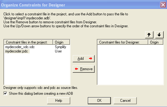
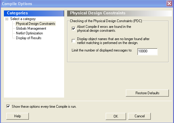
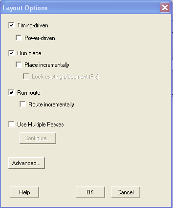
We are now ready to place and route using the Actel Designer Tool. Click on the Place and Route function block in project view. You will be prompted to add the constraint files to Designer. Select both add and click OK.
Designer will open.
First you are prompted to confirm the device type.
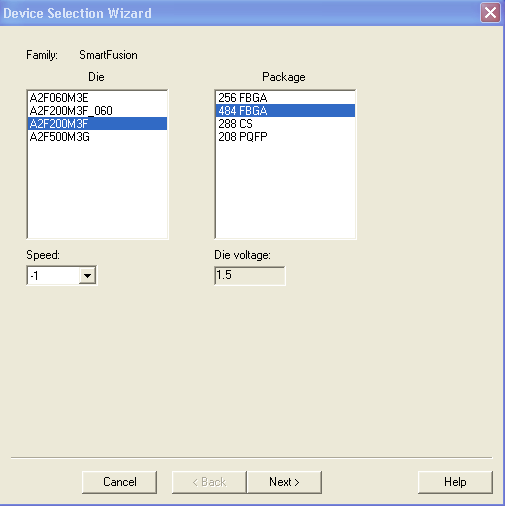
AsF200M3F and 484FBGA should be selected. Click next.

LVTTL should be selected for I/O Attributes.
Accept the window above and click finish. Click next and the designer window will appear.
The design flow window for place and route is shown graphically in the top view. Files for post layout simulation are created by clicking on the Back-Annotate icon. Click on the Back-Annotate button.
The following window will appear asking for confirmation to place the files in the project directory. Note yours will be in roughly the same path but in your student directory.
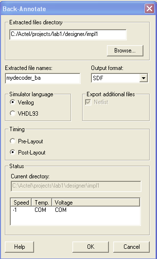
Accept the settings and click OK. The following window will appear.
Accept these settings and click OK. The following window will appear.
Accept these settings and click OK. Designer will now go into action and create the files. The following window showing all the processes in green should appear.
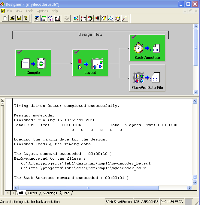
The post layout files are now available for simulation. The project however is still in a post synthesis state indicated by the icon in the top center of the project flow window.
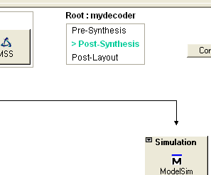
It must be in a post layout state before we can post layout simulate. To put the project in this state you must save the Designer adb file. You can either close Designer to do this or under File in Designer save. The state of the Project will now indicate Post Layout.
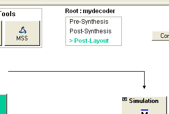
The Place and Route icon is also updated in project flow and the post Place & Route files are available to ModelSim.
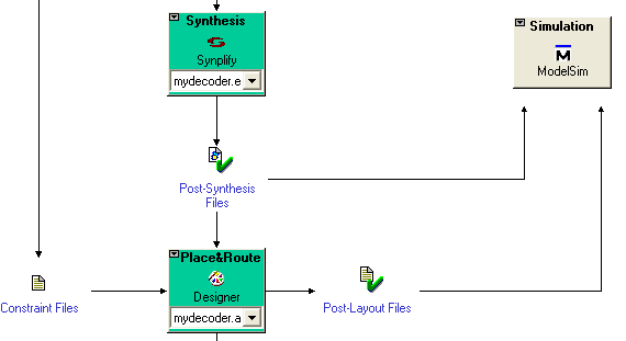
We are now finally ready to perform a post layout or timing simulation with ModelSim.
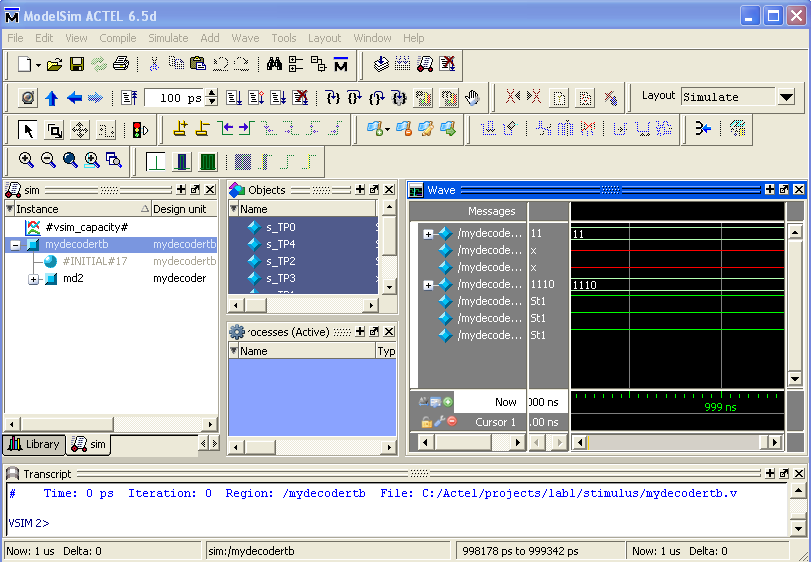
Click on the ModelSim icon to open ModelSim. All the necessary simulation files will be imported by the project manager and a ModelSim "do" file or command line script file will be created and executed. The following window will open with a simulation run for the previously written test bench in the waveform window.
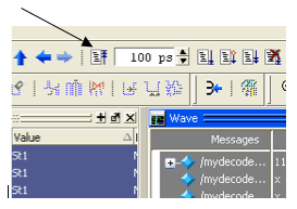
The test default time is 1000ns. To develop some basic ModelSim skills, let's run the simulation again. Click on the simulation restart.
The following window will appear.
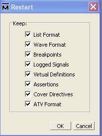
Click OK and the simulation waveform window will clear.
Change the simulation time by typing 100ns in the time window and then clicking the run button
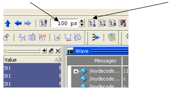
Adjust the waveform window and scroll to time zero. You can undock the window by clicking the undock icon in the waveform window.
Click on the waveform window and the cursor will appear (yellow line) then type the - sign (minus) to zoom out or + sign to zoom in. Adjust your display to show the decoder functions as follows.
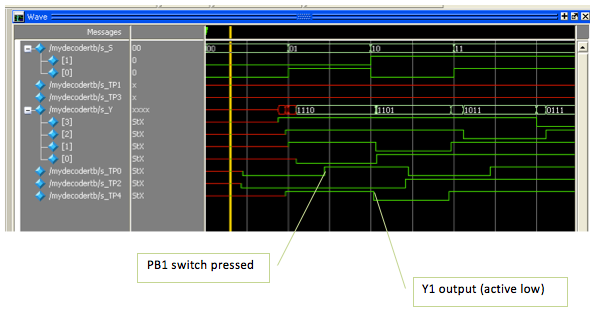
You can see the respective decodes (active low) for each coded input.
Remember, TP0 and T2 are connected to the push-button switches and the decoder input. TP4 is connected to Y1. Each vertical division is separated by 5ns so we are seeing about ~6ns of delay between the input and output.
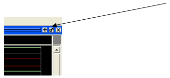
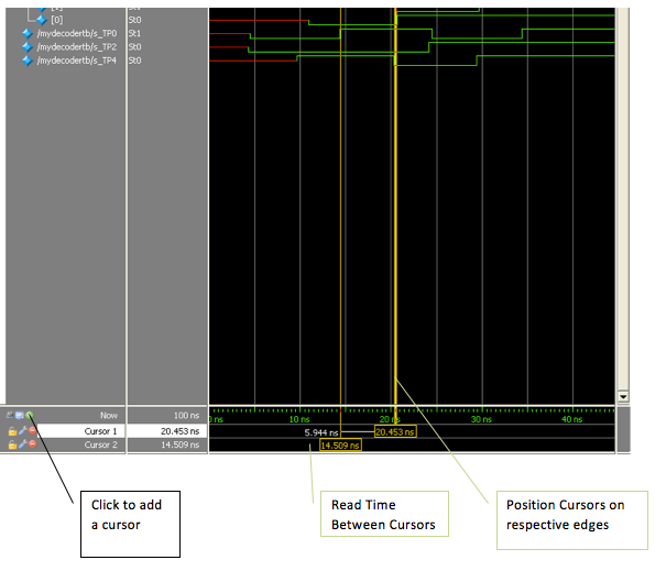
To measure the time precisely, you can add another cursor and position the cursors on each edge and read the value below. You can add cursors by clicking on the plus sign in the lower corner. See figure below.
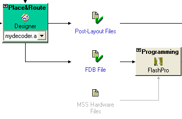
Finally a file must be generated that will be used to program the FGPA. In Designer click on the Flash Pro Data File Icon.
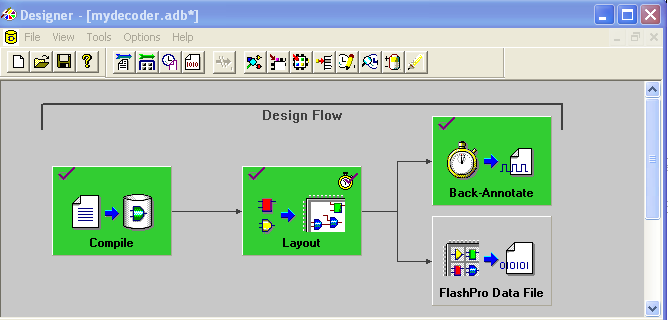
An FDB file will be generated in the tool chain. There are no MMS hardware files to program. Make sure the kit is connected. You will need to connect both USB ports on the kit to your computer. Click on the FlashPro Programming Icon
The following window will open.
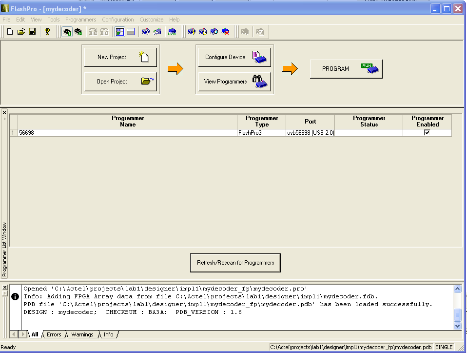
All the necessary information has been imported. Click on the Program button. The process will take several seconds and should indicate success when complete.
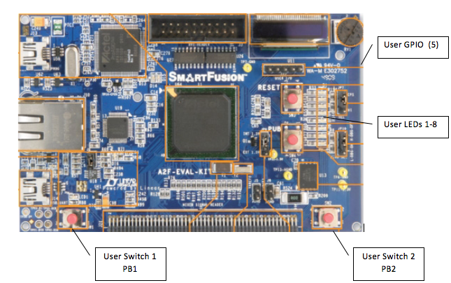
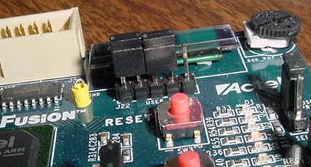
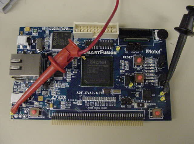
You will have to install the jumpers between GPIO 1 and 2 and between GPIO 3 and 4. Use the jumpers provided in the lab to do this. They also have the provision to install header pins on top to hook up probes for measurement.
Observe the LEDs on the kit. Notice the 4th led from the top is illuminated. This is output Y3 of the decoder. Remember, the switches are active low (when you push them they provide a logical zero). Push both switches and notice that Y0 is activated. Check the other decodes.
Each work station is equipped with a Agilent DSO3102A (digital storage oscilloscope, DSO). You probably used a scope like this in an introductory circuit lab to make basic measurements. Scopes are also very useful to verify and debug logic circuitry. Let's start with a brief review of the scope functions.
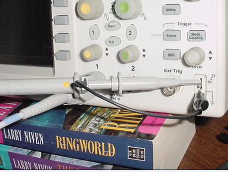
Connect a scope probe from channel 1 to the calibration output of the scope as shown in the following figure. The top terminal provides a 3Vpp (peak to peak) square wave at 1 KHz with a 1.5 volt DC offset. The bottom terminal is GND.
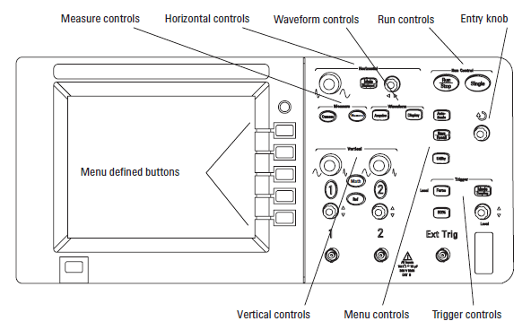
The scopes front panel controls are roughly categorized as follows.
Power On
Turn the scope on (lower left corner).
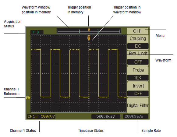
The scope has an auto scaling feature that works well with a stable signal like the calibration source. Try the auto scale and you should see a signal like the one above. The scaling feature will automatically adjust the display to best fit the calibration source signal. A waveform display should appear like the one bellow. The menu display will not appear yet.
The signal should have nice square corners as shown above. If not, the probes may need a compensation adjustment. There is a small slotted screw in the probe hear the GND jumper. Use a small screw driver and adjust until the corners are square. Omitting a probe compensation adjustment can contribute to measurement errors such as rise and fall times.
Activate channel 1 menu by pushing the number 1 button. The probe scaling will need to be set to 10x. These scope probes divide the signal by 10. The Auto adjust cannot detect the probe type, so it has to be done manually. If you use a straight BNC cable with clips, no signal division occurs and the scaling should be set to 1X. Generally you should use the scope probes when observing fast digital signals. Change the scaling to 1X and notice what the Channel 1 Status reads. Beware of this effect. It can cause confusion when trying to make sense out of a signal.
The large yellow knob is used to adjust the vertical gain. The lower left corner shows the scale in volts/vertical division (Channel 1 status).
The small yellow knob is used to adjust the vertical offset. Notice the ground reference point (little yellow arrow numbered 1 on left of display) will move with the adjustment.
Probe coupling can be set to DC, AC and GND. We will set it to DC for now. DC coupling couples both DC and AC components of a signal to the scopes input amplifier. AC coupling allows just the AC component in and with the DC components rejected. GND grounds the input so you can find the GND reference point if necessary. Set the input for GND and see where the ground reference is. If it is in the middle, the coupling was probably set to AC when you auto scaled. If it is near the bottom, the coupling was probably set to DC when you auto scaled. Play with the coupling and notice how the waveform changes position with or without the DC component (1.5 volt DC offset). Notice that the Channel status window indicates if the coupling is either DC or AC. Generally we will use DC coupling. However, sometimes AC coupling is very useful. AC coupling can be useful when trying to observe a very small AC signal on a large DC signal so that the gain can be increased without the DC component offsetting the waveform from display.
We will not use the BW or Digital Filter so just make sure they are OFF.
The large knob with grey center in the horizontal adjustment area controls the display time base. The scale is shown in the lower center window as time/horizontal division (TimeBase Status).
The scopes trigger synchronizes with the input signal and tells the scope when to start a display scan. The signal level that the synchronization is started from is the trigger level. Turn the small grey knob in the trigger display area (lower left) to adjust the trigger point. A horizontal yellowish line will appear on the screen and the waveform will sync (hold still) when it is in the vertical range of the signal. The point where the trigger level line intersect s the signal is the trigger point. Auto scaling will set the trigger level for the center of the signals vertical displacement automatically.
The scope can trigger on either the channel 1, 2 or an external source input located on the front panel (Ext Trig). Typically we will trigger on one of the 2 channels inputs. The Auto scale should have selected the active channel one. Try selecting channel 2 or external trigger and you should see the display loose synch and "free run".
Press the trigger mode button to evoke the trigger menu. Trigger slope selects if the scope is triggered on either a rising or falling edge. Notice that as you change the slope selection the trigger point indicator (small yellow arrow near top with T) follows slope selection.
Like the probe coupling the trigger can be AC or DC coupled. We will typically use DC coupling. Auto scale should set the coupling to DC typically.
Auto scale should have set Auto sweep mode. Auto sweep means the scope will trigger or display when no trigger is detected. This can be useful when you are initially adjusting the display and trying to "find" the signal. Adjust the trigger level until it is out of range of the signal. You should notice the display is active but the signal does not synch or will appear to "free run"
In manual sweep mode (called "normal mode" on our scopes), the scope will only display when the trigger is detected. Set the sweep mode to manual. Adjust the trigger level until out range of the signal. The display signal should disappear. When the trigger level is returned to the signal range, the display should reappear.
The scope will continue to display on each detected trigger edge in auto and manual mode. Sometimes it is useful to trigger on an edge just once. In manual mode, press the Single button in the upper right corner. It should trigger immediately if the trigger level is within the signal. The display is frozen or captured the event. Try adjusting the trigger level outside the display signal. Push single and adjust the level until it meets the signal range and you will see the scope trigger and capture the display. This is not a very interesting feature for this signal, but with single event signals it is very useful.
Auto scaling works well with a single source stable signal like the calibration source. It does not behave well with many signal types so beware that you may have to use manual adjustments to see or capture the signal.
The scope is probably the most versatile instrument on the workbench once you develop some confidence with one. If in doubt about your scope settings, hook the probe up to the reference output and make sure you understand what you are observing and how they correspond to your settings. Keep in mind that auto scaling does not always work. Get comfortable using the manual controls. There is much more this scope can do. You can read the user manual listed in the references for more info or just play with the scope. Also, vendors typically provide tutorials on their websites regarding various measurement applications from simple to complex.
Next we will measure the on chip propagation delay from the push button switch input to the Y1 output with the scope. Go back and take a look at the simulation waveform. Notice that we will have to trigger on the rising edge of test point 0 (push button 1 output) and observe the Y0 (active low) going low on test point 4. Clip the probe 1 on TP0 and probe 2 on TP4 as shown below. Attach the probe grounds as shown to ground test points provided on the kit. Take care not to touch other components and smoke something. Disconnect the power to the board (USB cable) to be safe. The FPGA will remain programmed.
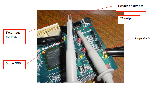
Make sure channels 1 and 2 are on and the settings are 2 volts per division, DC coupling and 10x probes. While the trigger mode is in auto, set the channel offsets so that both signals can be clearly seen. Set the trigger level adjustment as described above. Try pushing sw 1 and see the signal go up and down. To activate Y1 (channel 2) you must apply a binary 10 code or switch 2 depressed (active low) and switch 1 not depressed.
Let's see if we can capture the event of switch 1 going from low to high and the Y1 output becoming active (low) just like what we measured in the simulation. We will need to trigger on channel 1 (trigger source ch 1), slope rising and single event mode (manual and press Single button) and set the trigger level adjustment appropriately. To trigger you will have to make sure the trigger level is about 2 volts above channel 1 ground reference. Make sure the Single button is pressed (illuminated) to arm the scope. Press sw 1 and release and the scope should trigger. You may notice that nothing has happened in the Y1 output. That is because Sw2 is logical high.
We wish to capture the event SW2 low, SW1 low![]() SW1 high. To do this, both
switches need to be pushed down and then SW1 released. Arm the trigger
and try
again. You may need to push the switches before arming to avoid a false
trigger. Now you should see Y1 go low just after the rising edge of
SW1.
SW1 high. To do this, both
switches need to be pushed down and then SW1 released. Arm the trigger
and try
again. You may need to push the switches before arming to avoid a false
trigger. Now you should see Y1 go low just after the rising edge of
SW1.
We wish to see the propagation delay between SW1 high and Y1 going low. To do so we need to expand the time base. We know this is on the order of 6 ns. We will need to adjust the time base. It is not possible to adjust to the resolution we need after the capture. Arm the trigger (press Single) and adjust the time base for 5ns/division. Repeat the test. You should clearly see a delay on the order of 5ns.
Notice that it is not clear where to start and finish the delay measurement along the signal slope. We need to know the logic switching levels to make an exact measurement. Notice that you can also see a 2nd order response in the signal as it settles. The scope can be used to check basic logic functionality or can provide great amplitude and time resolution if needed. A screen shot of the SW 1 (top trace) and Y1 output (bottom trace) follows. You can see a propagation delay of about 1 division or 5ns.
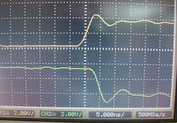
Notice that we are just about at the limit of the capability of this particular DSO. If higher frequencies, or even shorter propagation delays were to be observed, we would need a more expensive oscilloscope providing higher sampling rate and bandwidth.
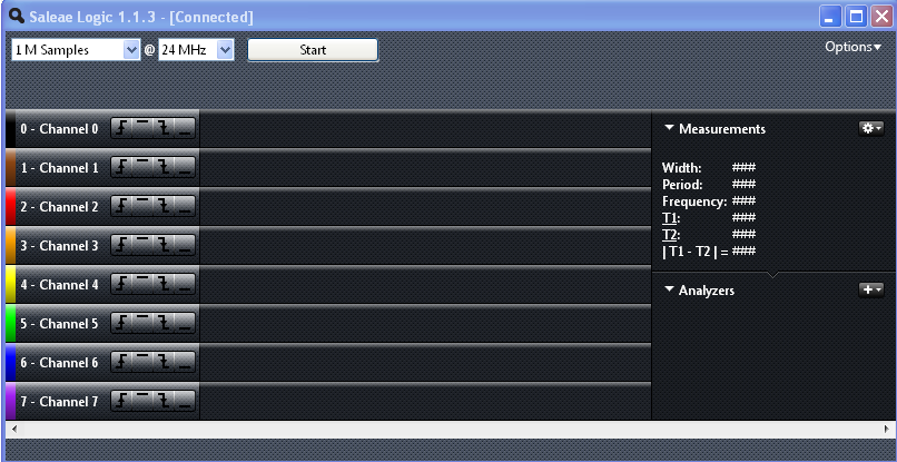
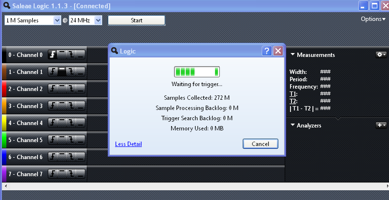
Each work station is equipped with an Agilent 16600A digital logic analyzer (DLA). This is a very sophisticated logic analyzer with the capacity to record and observe over 100 digital signals simultaneously! Logic analyzers with this sort of capacity can be complex to use and expensive usually exceeding $20k. Consequently, logic analyzers are not as common as oscilloscopes. Some low cost USB versions are now available. We will use one these USB logic analyzers for this lab. The Saleae logic analyzers can record and observe 8 channels simultaneously, trigger on complex conditions, decode various serial protocols and are easy to use for a mere $150.
Logic analyzers are used to verify logic functions by observing logical signals as we did with the oscilloscope. The big difference is that you can observe many more signals with a logic analyzer then you can with a basic 2 channel scope. The problem is you cannot observe the signals with the same vertical (voltage amplitude) or horizontal resolution (time). The logic analyzer classifies and then stores the input signal's amplitude as either a high or low. The Saleae's maximum sample rate is 24MHz providing a time measurement resolution of about 0.1us. Remember, with the scope we could resolve propagation delays to about 1ns. Depending on the application, these measurement resolutions are tolerable when observing basic logic function and when time measurements are much greater than 0.1us.
While DLAs like the 16600A are complex to set up and use, the USB based Saleae is quite simple.
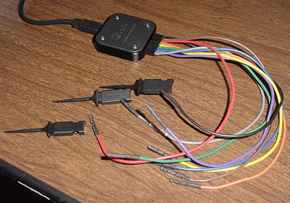
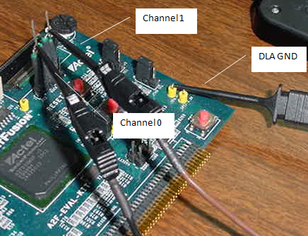
The Saleae DLA is powered via the USB connection, so simply plug it in. Note: the analyzer does not work thru the display USB port. The analyzer is quite compact with one USB connection and a probe pod consisting of 8 signal wires and a reference or GND connection. Each probe has a socket connector on the probe end that be connected into common circuit board headers or grabber clips supplied with the kit.
The Saleae application program can be evoked from the following desktop ICON or from the program list.
A following window should appear.
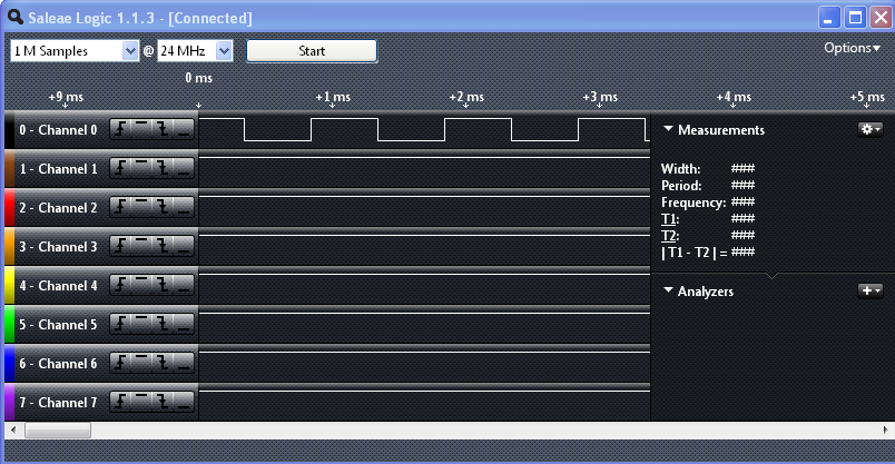

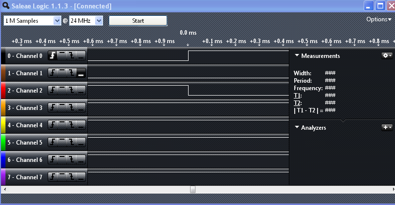
Likewise, triggering can be logical level 0 or 1 sensitive. This is the display for a positive level trigger.
Each workstation is equipped with an Agilent digital multi-meter (DMM). The meter is used for general measurements including: voltage, current, resistance and capacitance. These should be relatively familiar to you from introductory lab courses.
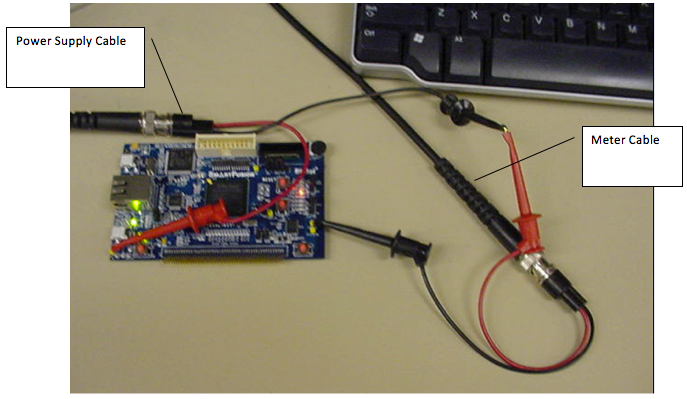
For a simple application, let's measure the power drawn by the kit. We can model the kit as a load resistor for this measurement. By measuring the voltage across the kit and the current supplied we can determine the power load. Voltage to the kit is provided through the USB cable. We could cut the USB cable so we could measure the power, but that will be a bit messy. Instead, let's us the lab power supply.
Before hooking anything up, adjust the power supplies 6V output to be 5.00 volts. Note you have to have the Output turned on.
Disconnect the USB cables from your kit. Get a BNC cable, BNC grabber adapter and BNC to banana adapter.
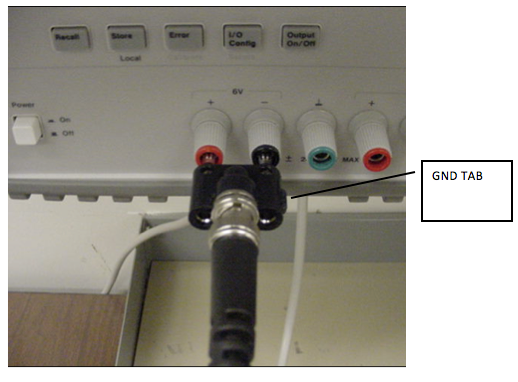
TURN OFF THE POWER SUPPLY OUTPUT
TAKE CARE TO CONNECT THE BANANA TO BNC CONNECTOR WITH THE GND TAB ON THE GROUND TERMINAL OF THE POWER SUPPLY. FAILING TO DO THIS WILL APPLY NEGATIVE VOLTAGE AND FRY THE KIT!!
Next, connect the red clip to the kits 5 volt supply test pin and the black clip to a GND test pin.
Turn the power supply kit output on and you should be able to observe the current supplied to the kit. The power supply current meter is accurate for currents >10ma. Let's check it. Get another cable like the one you used to hook the power supply to the kit. Attach the cable to the DMMs current terminals.
The adapter ground ref tab orientation is not critical. It will only effect the current flow reading direction (+/-). Next place this cable in the ground path of the power supply cable like this.
Observe the difference. At this current level the power supply meter should be very accurate. In most cases the power supply meter is adequate.
The best way to make sure you understand this lab is to try another hardware implementation. Create another project. Implement a binary-to-unary encoder that treats the switches as binary-weighted inputs (SW1 2^0, SW2 2^1) and provides an output that lights the appropriate number of LEDs. Pick any set of 3 LEDs. Having no buttons pressed (binary "11") should result in no LEDs being illuminated, having only sw1 pressed should have the first LED illuminated, only pressing sw2 should have the first two LEDs illuminated, and pressing both switches should have all three LEDs illuminated.
    SW2             SW1           Number LEDs on
=============   =============     ==============
not pressed     not pressed             0
not pressed     pressed                 1
pressed         not pressed             2
pressed         pressed                 3
Remember the LEDs and the switches are active low. When you push the switches they produce a logical 0. A LED is illuminated when a logical 0 is applied.
Measure the propagation delay at the kit IO pins for the encoder inputs going from (SW1 = pressed, SW2 = not pressed) to (SW1 = not pressed, SW2 = not pressed) and the associated LED changing illumination status. Measure in simulation and on the kit with the scope. Your simulation and kit measurements should be within 1-2ns of each other. You must measure the propagation delay in simulation from input pins to the output pins of the FGPA to be comparable to the oscilloscope measurement. You should be able to use In-Lab test bench for the simulation with a minor modification.
You may work with a partner for this assignment if you worked solo for the In-Lab. If you don't have a partner after this lab, consider finding one by 2nd lab. The labs will become increasingly difficult and you will need the help.
Submit the following for the Post Lab Assignment.
You will be given a keypad entry code to the lab so you can use the lab any time except when other lab sections are meeting. Be sure and read the unsupported lab policy before using the lab. There are important lab safety issues documented in the policy. There will also be some supported lab open hours if you need additional help. See the course web page for times.