Variable capacitors (varactors) are essential components in tunable microwave circuits. Ferroelectric materials, which allow for its permittivity being adjusted by the electric field applied, are legitimate candidates for varactors. Among them, barium strontium titanate (BST) has been used in various microwave circuits, such as filters, phase shifters, and matching networks, to provide the benefit of tunability. Compared to microelectromechanical systems (MEMS) varactors, thin-film BST capacitors exhibit a higher tuning ratio under relatively low biasing voltages. However, due to the inherent nonlinear nature of the ferroelectric materials, linearity has been a concern, especially for high power applications and spectrally-packed communication systems.
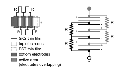
Linearity improvement can be achieved through the proper design of the device architecture, rather than changing the base material. While previous researchers have proven the effectiveness of architectural approaches for gap capacitors, in this work, a simple method to reduce the nonlinearity of parallel plate capacitors is suggested. This work presents an analysis of the technique for the study of tradeoffs and optimization of BST varactor-based circuits for wireless communication applications. The device architecture is illustrated in with a 5-stacked example. Five capacitors are connected in series through top and bottom electrodes alternatively. Thin-film resistors link together top or bottom electrodes respectively to ensure that the bias voltage falls on each capacitor equally.
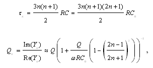
Through analysis the effects of number of stacked capacitors and the biasing resistors on the quality factor and the tuning speed of the composite capacitor are found. The time constant and the quality factor can be describe by equations
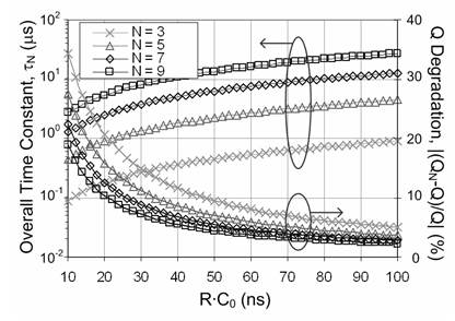
respectively, where N = 2n+1 is the number of elements. The tradeoff between time constant and the degraded quality factor can be plotted versus RC0 for composite capacitors with various Ns.
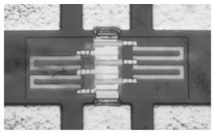
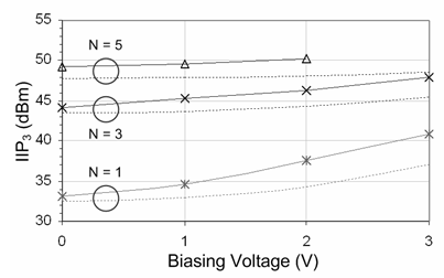
The The BST capacitors were fabricated on 430-mm-thick sapphire. The substrate has a dielectric constant of 9.39 as the electric field is perpendicular to its C-axis. The bottom electrodes composed of Ti/Au/Pt (20/2000/1000 Å) were formed first. BST thin-film was then deposited using Pulse Laser Deposition (PLD) technique with 50/50 BST target. The measured film thickness was 400 nm. The top electrodes composed of Pt/Au (1000/2000 Å) were then formed. After that, BST thin-film was etched in the regions other than the active area. Thin-film SiCr lines with thickness of 100 nm were then sputtered. Following that, the metal contacts composed of Cr/Au (200/500 Å) were formed to connect the biasing resistors to the electrodes and serve as the bottom electrodes of the metal-insulator-metal (MIM) capacitors in other regions. Silicon nitride (Si3N4) thin-film, serving as the dielectric layer in the MIM capacitors and also the passivation for the BST capacitors, was deposited using Plasma Enhanced Chemical Vapor Deposition (PECVD) technique. The film thickness was measured to be 1300 Å. Finally, the other metal traces were electroplated with gold to around 8 mm. The photograph of a 5-stacked capacitor is shown. The device area of this capacitor is 350´160 mm2, including the biasing resistors and the passivation layer. The capacitance of it is around 1.4 pF at zero bias. Various measurements are performed to demonstrate the efficacy of the technique. The 3rd order intercept point at input (IIP3) is found to be improved by 16 dB. The hot-tuning test shows that the tunability is maintained for up to 20-V peak-to-peak swing.
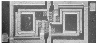
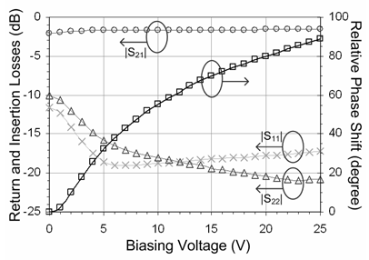
A phase shifter was designed based on all-pass network, where BST capacitors utilizing the proposed architecture with N = 5 were employed. The circuit was laid out in a flipped sense to reduce the area and facilitate cascading with other circuits. The photograph of the fabricated circuit is shown. Due to fabrication errors, the inductances of the spiral inductors were deviated from the expected value. After trimming with bond-wires, the phase shifter was measured. Its small-signal response at 2.4 GHz is shown. The insertion loss was less than 2 dB and the input and output return losses were greater than 10 dB. The relative phase shift over 0 to 25-V bias voltages was about 90 degree. The center frequency and frequency spacing of the two-tone signals for measuring the intermodulation distortion of the phase shifter were 2.4 GHz and 1 MHz, respectively. The IIP3 observed was greater than 40 dBm.
[1] J.-S. Fu, X. A. Zhu, J. D. Phillips, and A. Mortazawi, Improving linearity of ferroelectric-based microwave circuits, IEEE Trans. Microwave Theory & Tech., vol. 55, no. 2, pp. 354-360, February 2007.
[2] J.-S. Fu, X. A. Zhu, D.-Y. Chen, J. D. Phillips, and A. Mortazawi, A linearity improvement technique for thin-film barium strontium titanate capacitors, in 2006 IEEE MTT-S Int. Microwave Symp. Dig., June 2006.
