In previous published papers, several narrow-band multiple-device power amplifiers based on an extended resonance power combining technique have been reported. Power combining efficiencies up to 90% have been achieved at X and Ka bands. The extended resonance technique effectively places devices in shunt to combine the power from each active device. Since the magnitude of the voltage at each transistor is the same, the gain of the extended-resonance combining amplifier with N active devices is equal to the gain of a single-device amplifier, while its power capability is increased by N times. The significance of extended resonance technique lies in its ability to equally divide and combine the power of many devices using short length of transmission lines. The resulting circuits have compact layouts and are suitable for monolithic integration. However, due to these designs resonant nature, their 3-dB bandwidth is limited to 5%. It is the purpose of this work to demonstrate an extended-resonance combining based amplifier with broadband performance.
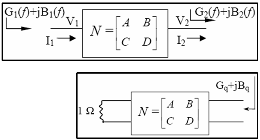
As shown by Carlin and others, when one port of a two-port lossless lumped-element network is terminated with pure resistive load, this networks layout can be determined from the rational function of the input Thevenin impedance (Zq=Rq+jXq) or admittance (Yq=Gq+jBq) at the other port. Another important theory about the lossless lumped-element network is that the rational function of Zq and Yq can be derived from their real parts Rq and Yq functions respectively by using Brune-Gewertz method. For lossless and reciprocal network N, through some simple derivations, it can be shown that the A and B elements of the networks transfer matrix are directly related with its Gq function. Therefore, when the complex admittances
(G2(f)+jB2(f)) are known, the values of A and B can be determined. Then based on A and B, we can determine the networks Gq function, and accordingly derive the rational function of Yq. In this way, the optimized lumped-element network layout with equal voltage distribution over the bandwidth of interest can be obtained. For the combining circuit presented in this paper, four-element low-pass ladder networks have been used.
Fig. 1. Two port network
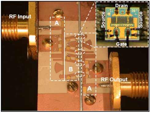
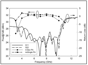
The designed 4-device broadband power amplifier was fabricated on Rogerss 25-mil-thick TMM6 and placed on an aluminum block that also served as a heat sink. The shunt capacitors with values smaller than 0.5 pF were realized by microstrip open-end stubs and radial stubs, while the larger capacitances were achieved by using single layer chip capacitors from Dielectric Laboratories Inc. Via-holes filled with 10-mil copper wires and multiple 1-mil aluminum bonding wires were used to connect the chip capacitors to the ground. Figure shows the perspective view of the fabricated 4-device amplifier with an enlarged view of the PHEMT transistor LP1500. The gate, drain and source of the transistor were respectively connected to the RF circuits and the ground through 1-mil aluminum bonding wires. Large signal measurements were performed on both power amplifiers from 3 to 10 GHz. The measured output power levels at 1-dB gain compression (Pout@1dB) over the bandwidth are plotted. The Pout@1dB from the single-device PA is multiplied by 4 times to illustrate the possible power level from an ideal combiner. The measured Pout@1dB from our design is around 31.9 dBm with 1-dB fluctuation from 4 to 9 GHz. A comparison of these data indicates the PCE for our design is around 90% from 5 to 9 GHz.
Fig. 2. Power Amplifier Fig. 3. Output power @1dB
