Miniature High-Impedance On-Chip Antennas
Wonbin Hong, N. Behdad, M. Flynn, and Kamal Sarabandi
|
|
|
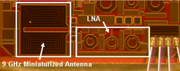
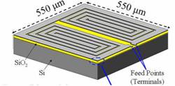
Miniaturized 9GHz slot antenna fabricated using
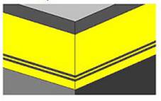
0.13mm CMOS process. (Left) Expanded view of the wafer corner showing two
parallel ground plane each 0.6 mm thick separated by 0.6 mm (M4 and M5).
This project entails
the design and demonstration of miniaturized antennas with the possibility of
achieving complete integration with the RF front end, and ultimately achieving
a single-chip wireless system. The antennas need to be placed above ground
plane which limits their radiation efficiency and reduces the bandwidths. Reducing
the size, increasing the bandwidth, and improving the efficiency of the antenna
in the presence of the ground plane are problems that will be addressed.
This
project has three main phases: first, to design a miniaturized antenna without
a ground plane and with a fairly high efficiency to conserve as much power as
possible; second, enhancing the bandwidth of the miniaturized antenna and
increasing the input impedance of the antenna so that it can be matched to a
very high impedance, and finally, the radiation efficiency of the antenna in
the presence of a ground plane must be enhanced. The first task is fulfilled
knowing that by a virtual enforcement of the required boundary condition at the
end of a slot antenna, the area occupied by the resonant antenna can be
reduced. Furthermore, loading the antenna with distributed inductors also
reduces the antenna size. Combining these two techniques, results in a highly
miniaturized slot antenna. Different bandwidth enhancement techniques that
increase the BW while maintaining the size have also been demonstrated.
Miniaturization of the antenna will be achieved via alternative slot antenna geometries, for which the antenna impedance can be varied (and matched to any RF input) by attaching the RF front end circuit at the proper slot location. Design and fabrication of an on-chip antenna using 0.13mm CMOS process was demonstrated. To archive optimum overall energy, tradeoffs between digital, analog and mixed-signal signal processing will be investigated.

Prototype integrated
antenna and LNA in 130nm CMOS.
Integration of the antenna on-chip not only
reduces size of the complete transceiver by more than an order of magnitude,
but also offers new opportunities for system optimization. Because of
silicon-substrate and metal interconnect losses, an on-chip antenna is less
efficient than a conventional one, however on the other hand, an on-chip
antenna gives more system design freedom. The input impedance need no longer be
limited to 50 W , in fact our initial
work indicates that an impedance of 80W
is optimum. The use of an on-chip antenna eliminates RF board and RF connector
losses. Since the antenna signal no longer passes through an I/O pad to the LNA
input, electro-static discharge (ESD) protection can be eliminated from these
sensitive nodes further reducing loss.


