
Copyright © 2010 -
Ye-Sheng Kuo,
Thomas Schmid,
Matt Smith,
and Prabal Dutta.
See posted lab schedule for due dates, in-lab, and post-lab due dates.
As you might guess, with all the other goodies included in SmartFusion MSS the folks at Actel did not forget ADC and DAC resources. The MSS ACE (Analog Computing Engine) is relatively complex component providing DAC/ADC functionality, sampling control, analog threshold detection, filtering and DMA access just to mention a few. Despite this apparent complexity, the ACE can be relatively easy to use. The ACE like the other MSS components is automatically interfaced to the peripheral bus and a user friendly GUI is provided for configuration.
The purpose of this lab is to...
Quantizing error is inherent in most measurements and limits the certainty a measurement. The quantizing error for an ADC is defined to be 1 LSB. It can also be expressed in volts or LSBv for an n-bit ADC .
Quantizing error in volts = voltage range of conversion/2^n
For our converter, the voltage range is 2.56 volts. If we program the ACE to be an 8 bit ADC, the quantizing error in milli-volts will be
LSBv = 2.56 volts/2^8 = 10 mv
So, you can only know the value to 10 mv. The ideal quantum size of 1 LSB can actually vary to be larger or smaller from fabrication issues and other sources. These effects are characterized as integral non-linearity (INL) and differential non-linearity (DNL). Under normal conditions in the lab you will NOT observe this.
Plotting the conversion value against the analog value defines the ADC transfer characteristic or input to output relationship.
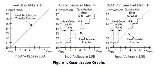
The first graph shows the ideal transfer function excluding quantizing effects. The second case illustrates the affect of quantizing resulting in a stair case like transfer function. In this case the quantization error is from 0 LSB to 1 LSB. The last graph illustrates an ADC model that shifts the transfer function to center the quantizing error over the conversion intervals. In this case, the quantization error is +/- ½ LSB. In both cases the quantizing error is 1 LSB, but the relationship of the conversion value to the input voltage is shifted by ½ LSB.
When converting relatively stable voltages to digital values a few samples are sufficient to represent the voltage. However, when sampling time varying signals the question arises, just how many samples are required to represent the signal. The Nyquist-Shannon sampling theorem predicts that periodic signals can be reproduced when the original signal is sampled at >= 2 times its period. If the signal is sampled at a rate that is less than the 2 times its period, the reconstructed signal will have a different frequency and shape. A simple predictor is given by the following equation:
alias frequency = sampled signal frequency - sampling frequency
The reconstructed signal is commonly referred to as an alias and is a common problem in applied signal processing. There are many topics forming the foundation of signal processing, but these basics should cover our needs for the present.
Each SmartFusion Eval Kit has 10 direct analog input channel and 2 Sigma-delta DAC. We want to use just one of each. Open the Libero, SmartDesign. Double click ACE
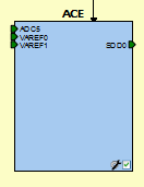
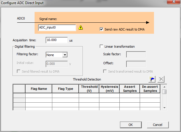
In left column, add a ADC Direct Input service. Put ADC_input0 in Signal Name and check Send raw ADC result to DMA, and click OK. On the top of configurator, set the resolution to 8 bits.
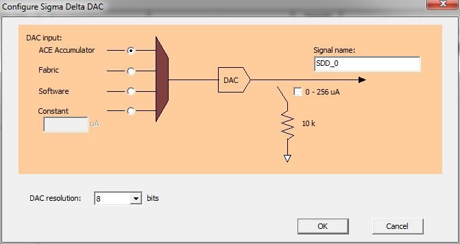
Add another Sigma Delta DAC service, select ACE Accumulator as DAC input and select the DAC resolution to 8 bits. Click OK.
Set your ADC Direct Input Package Pin to V12 ( ADC5 ), and
Sigma Delta DAC Package
Pin to V7 ( SDD0 )
Go to Controller tab, select ADC1_MAIN. Add all Available
signals to sampling rate requirement. Click Calculate Sequence and
Actual Rate
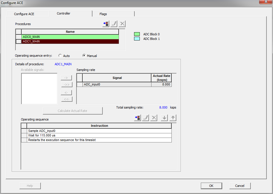
Notice that the Total sampling rate should be 87.000 ksps. We
want to slow it down to 8 ksps.
Select the Operating sequence entry to Manual and insert a
operating sequence slot.

Insert a WAIT TIME and configure it to 115us. Move the Wait for 115.00us above Restarts the execution sequence for this timeslot. Click Calculate Actual Rate. The Actual Rate for ADC / DAC should be 8.000 ksps. Click OK and go to Firmware tab. Check the UART, ACE, NVM, PDMA drivers.
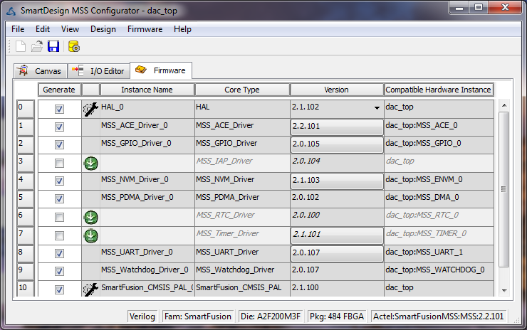
Click Save and Generate. Put the IP core to canvas and run the synthesis, place & route and flash your SmartFusion.
Create a C project in Softconsole as you did before, set the linker
script, import the drivers. The following code reads the ADC
and write the DAC with the ADC conversion value
#include <stdio.h>
#include <inttypes.h>
#include "drivers/mss_ace/mss_ace.h"
#include "drivers/mss_uart/mss_uart.h"

ace_channel_handle_t adc_handler;

int main(){
    ACE_init();
    ACE_configure_sdd(
    	SDD1_OUT,
    	SDD_8_BITS,
    	SDD_VOLTAGE_MODE | SDD_RETURN_TO_ZERO,
    	INDIVIDUAL_UPDATE
    );
    ACE_enable_sdd(SDD1_OUT);

    adc_handler = ACE_get_channel_handle((const uint8_t *)"ADC_input0");

    while(1){
    	uint16_t adc_data = ACE_get_ppe_sample(adc_handler);
    	ACE_set_sdd_value(SDD1_OUT, (uint32_t)(adc_data>>4));
    }
    return 0;
}
Put the code in a main.c file. Compile the source code and launch the debugger session.
Hook the signal generator to the extension board header pin 5 ( paper label) in the bottom right corner to provide input to the DAC. If you don't have a paper label this is labeled ADC1. Observe the DAC output on the BNC shown connected.
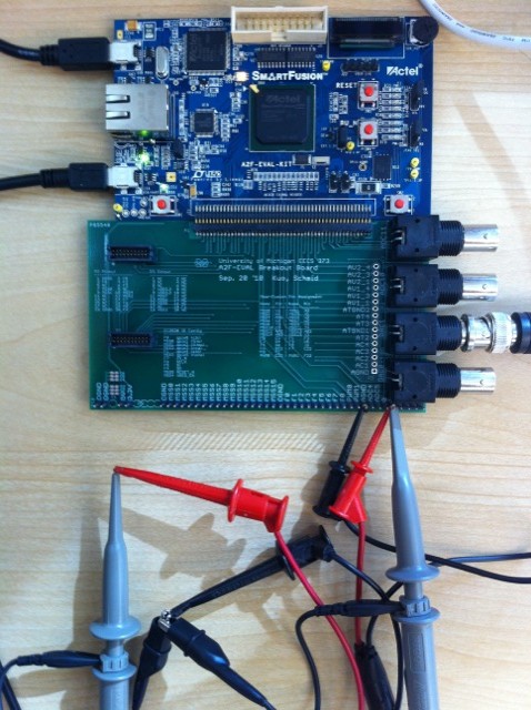
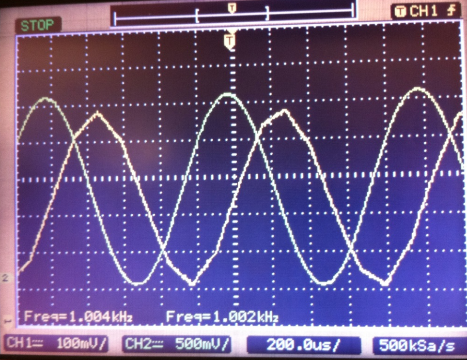
Using the signal generator as a signal source, provide a sine wave that centers a sine wave over the input range of the ADC (0 - 2.56 volts). A DC offset of 1.25 volts should be fine with a Vpp (peak to peak) voltage of 2.5 volts. Be sure the signal generator output is set to High Z to insure accurate signal levels. Verify with the scope before attaching to the kit to avoid damage to the ACE.
Set the source signal to 1 KHz sine wave. Observe the DAC output. Notice the quantizing steps in the output wave form. With the input and output waveforms displayed on the scope, it should look something like this.
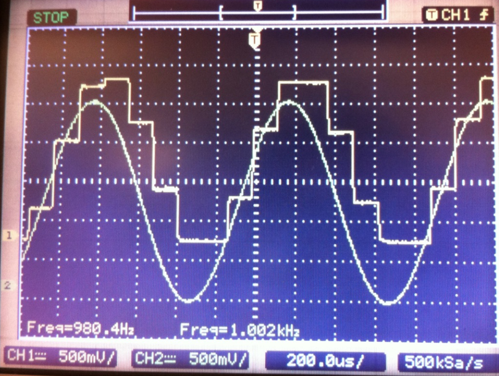
For the post lab, record the number of quantizing steps there are per cycle.
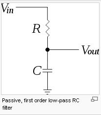
Construct a low pass filter with a 1K ohm resistor and 0.068uf capacitor on a protoboard. Wire the DAC to the input of the filter and observe the output.
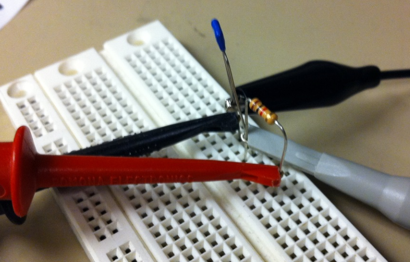
You should notice a signal that is pretty close to a continuous sine wave. The signal will be attenuated because of the filter.
The filter output amplitude should be about 0.707 the value of the input voltage value at the 3db down frequency (2.34KHz) . Notice that it is considerably lower. Adjust the frequency until the filter output value is 0.707 the value of the source frequency and record the frequency for the post lab.
printf("adc_result: %u\r\n", (adc_data>>4));
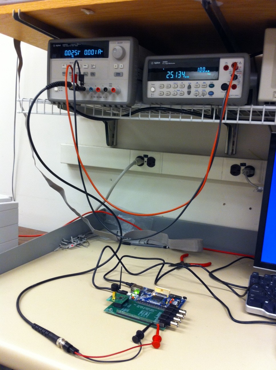
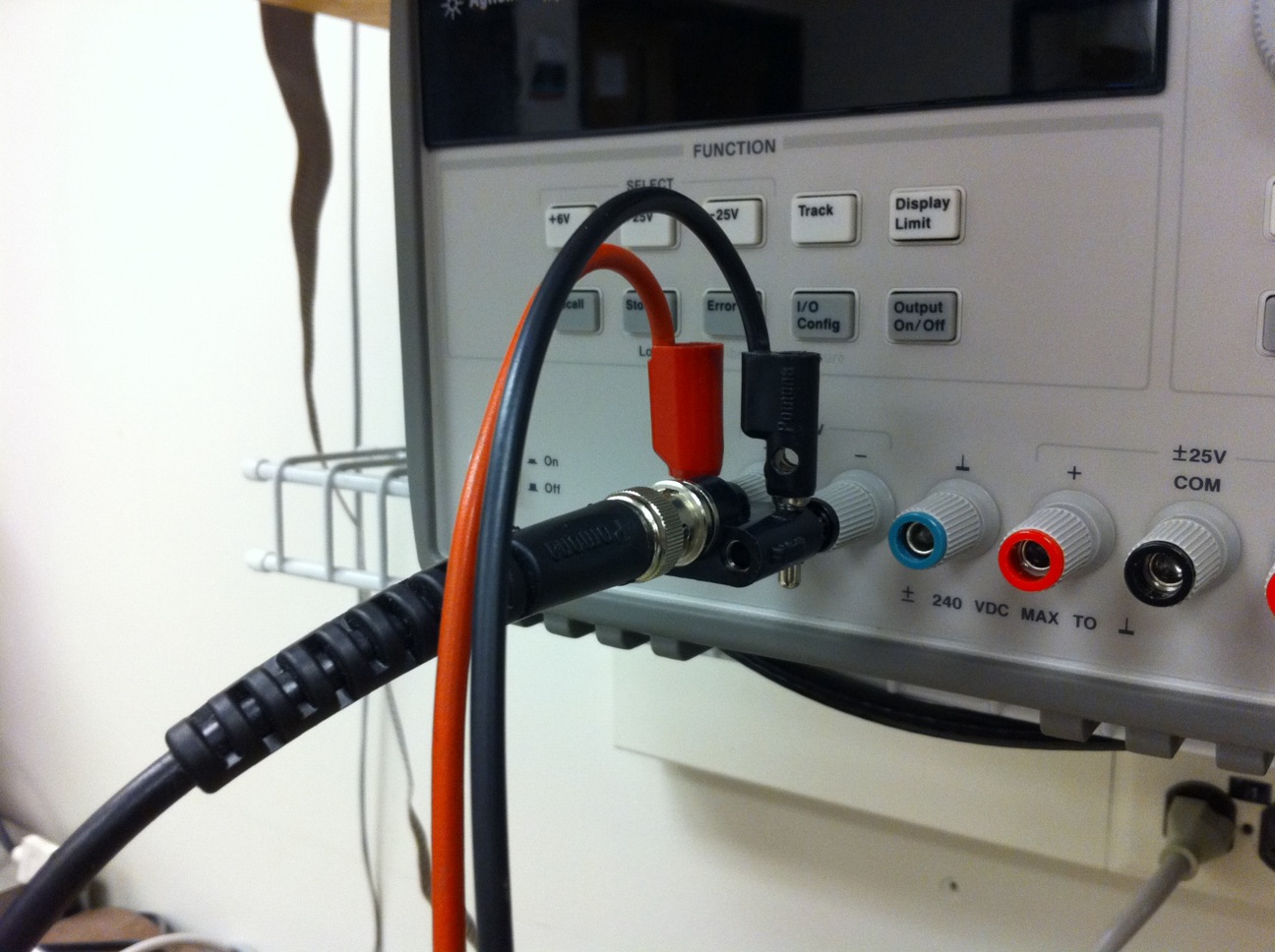
You will measure the transition or boundary voltages for the first 4 ADC conversion values 0, 1, 2 and 3. The lab power supply 0-6 volts output can be adjusted to ~ 1mv, so you can use this as a voltage source. The voltage meter on the power supply is not accurate enough for 1 mv measurements, so you should use the DMM. Be sure to use the cable configurations shown in the following configuration or you will introduce interference that will make it difficult to resolve the transition voltages.
The procedure for measuring the transitions voltages is to simply start at 0 volts then gradually increase the voltage until you see the conversion value change. The voltage at which the conversion value changes Is the transition voltage. You will likely find that the transition voltage does not occur neatly on a 1mv boundary. In fact, it will waggle between adjacent conversion values for several millivolts. Measure this transition phase by measuring when the waggling starts and stops. Record the following values to answer questions in the post lab assignment. The start and end boundary values should be no more than a few millivolts apart. If they are, consult your lab instructor.
| Conversion Value | Low Boundary Start (mv) | Low Boundary End (mv) | High Boundary Start (mv) | High Boundary End (mv) |
|---|---|---|---|---|
| 0 | 0 | 0 | ||
| 1 | ||||
| 2 | ||||
| 3 |
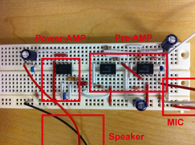
Now, we learned how to use ADC / DAC in SoftConsole, we want to build a voice recorder using the SmartFusion Eval. Kit. However, we cannot connect the microphone directly to the ADC and connect the speaker to DAC. We need some signal conditioning between the board and mic / speaker.
You should received the following components in this lab.
| Components | Value | Quantity |
|---|---|---|
| Breadboard | 1 | |
| MIC | 1 | |
| Speaker | 1 | |
| OP Amp | LM741 | 2 |
| Power Amp | LM386 | 1 |
| Resistor | 10 Ω | 1 |
| 1k Ω | 1 | |
| 2.2k Ω | 2 | |
| 10k Ω | 2 | |
| 22k Ω | 2 | |
| 100k Ω | 1 | |
| Capacitor | 0.047uF | 1 |
| 0.068uF | 2 | |
| 0.47uF | 1 | |
| 220uF | 3 |
We want to implement the voice recorder system. The system is composed of three parts,
Before building your circuit, you may want to check these references.
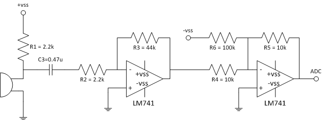
The following circuit is for your reference. Keep your connections short and neat as shown.
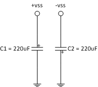
Once you are done with the Pre-Amp part, connect the power supply to the board. In this circuit, we need +/- 10 Volt for +/- VSS. Be careful not to short the power to ground. If you notice the current goes thru the roof, turn off the output of power supply! This usually means your circuit has a short between power and gnd. Connect the scope to the Pre-Amp output and the microphone(positive), observe the amplified signal. What is the gain(Vout/Vin) of the circuit? Do not need to consider the DC offset, which means you can set the scope to AC coupling to observe the gain.
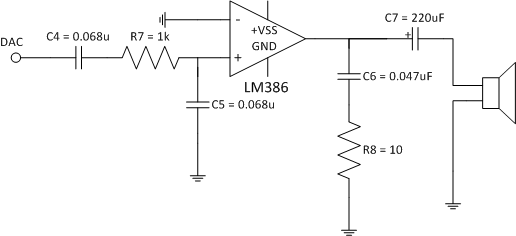
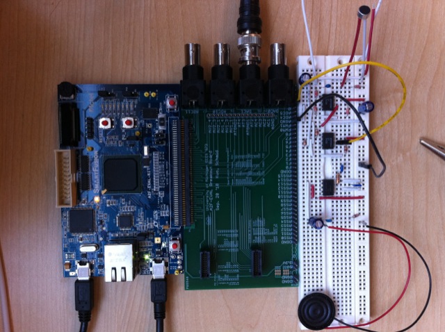
When you finish the Power-Amp part, do not connect to the SmartFusion kit immediately. Instead, verify the operation of the by connecting the first part and second part together. Try to generate some voice in MIC. Can you hear the voice from speaker? If not, check the circuit until you can hear your voice in the speaker.
Connect the pre-amp output to the ADC1 as you did before, and DAC1 output to power-amp. In this typical application, we will record voice for 10 seconds to memory. The size of the data = 8k Samples/sec × 1 Byte/Sample × 10 sec = 80k bytes. We are memory limited at the moment and have to share the space with the program code.
The data is stored in 0x6002b000, if you put your code in eVNM, make sure the data won't override your code
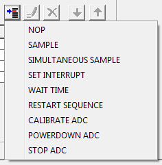
Open the Libro, we want to configure the ACE with interrupt telling the
microprocessor the DAC data has been sampled. In other words, we want
to generate the 8K Hz interrupt and update the DAC registers. Go to the
controller tab, insert operation sequence slot, select SET
INTERRUPT
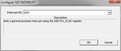
Configure the interrupt bit to GP0, click OK.
Generate the design, synthesis and program your SmartFusion. Updating the following code to SoftConsole. Find out how to subscribe the interrupt generated by ACE. (PC0_FLAG0) Update the DAC data once the interrupt is fired.
#include <stdio.h>
#include <inttypes.h>
#include "drivers/mss_uart/mss_uart.h"
#include "drivers/mss_watchdog/mss_watchdog.h"
#include "drivers/mss_ace/mss_ace.h"
#include "drivers/mss_gpio/mss_gpio.h"
#include "drivers/mss_nvm/mss_nvm.h"
#include "drivers/mss_pdma/mss_pdma.h"

uint8_t *envm = (uint8_t *) 0x6002b000;
uint32_t envm_idx;

#define FREE_BUFFER         	0
#define UNDER_DMA_CONTROL   	1
#define DATA_READY          	2
#define SAMPLES_BUFFER_SIZE	128
#define NB_OF_SAMPLE_BUFFERS	2
#define	TOTAL_SAMPLE_SIZE	81920

/* PDMA  destination */
uint32_t samples_buffer[NB_OF_SAMPLE_BUFFERS][SAMPLES_BUFFER_SIZE];
uint8_t buffer_status[NB_OF_SAMPLE_BUFFERS];

void ace_pdma_rx_handler();
void process_samples();
void free_samples(uint8_t);
void play_samples();

volatile uint8_t pdma_buffer_idx = NB_OF_SAMPLE_BUFFERS;

int main()
{
    uint8_t full = 0;
    envm_idx = 0;
    dac_irq = 0;

    MSS_WD_disable();
    ACE_init();
    ACE_configure_sdd(
    	SDD1_OUT,
    	SDD_8_BITS,
    	SDD_VOLTAGE_MODE | SDD_RETURN_TO_ZERO,
    	INDIVIDUAL_UPDATE
    );
    ACE_enable_sdd(SDD1_OUT);


    PDMA_init();
    PDMA_configure
    (
        PDMA_CHANNEL_0,
        PDMA_FROM_ACE,
        PDMA_LOW_PRIORITY | PDMA_WORD_TRANSFER | PDMA_INC_DEST_FOUR_BYTES,
        PDMA_DEFAULT_WRITE_ADJ
    );
    PDMA_set_irq_handler( PDMA_CHANNEL_0, ace_pdma_rx_handler );

    NVIC_EnableIRQ( DMA_IRQn );

    free_samples(full);

    while (1)
    {
	// recording mode
    	if (full==0)
	   process_samples();
	// playing mode
    	else{
	    play_samples();
    	}

    	if (envm_idx>=TOTAL_SAMPLE_SIZE){
    		envm_idx = 0;
    		if (full)
    			full = 0;
    		else
    			full = 1;
    		free_samples(full);
    	}
    }
    return 0;
}

void free_samples(uint8_t full_flag){
	uint32_t i;
	for ( i = 0; i < NB_OF_SAMPLE_BUFFERS; ++i ){
		buffer_status[i] = FREE_BUFFER;
	}
	pdma_buffer_idx = 0;
	buffer_status[pdma_buffer_idx] = UNDER_DMA_CONTROL;
	if (full_flag){
	}
	else{
		PDMA_enable_irq( PDMA_CHANNEL_0 );
	    PDMA_start
	    (
	        PDMA_CHANNEL_0,
	        (uint32_t) PDMA_ACE_PPE_DATAOUT,
	        (uint32_t) samples_buffer[pdma_buffer_idx],
	        SAMPLES_BUFFER_SIZE
	    );
	}

}

// PDMA recived interrupt
void ace_pdma_rx_handler()
{
    PDMA_clear_irq( PDMA_CHANNEL_0 );
    buffer_status[pdma_buffer_idx] = DATA_READY;
    PDMA_disable_irq( PDMA_CHANNEL_0 );
}

void process_samples(){
    uint8_t i;
    if ( buffer_status[pdma_buffer_idx] == DATA_READY){
    	uint32_t proc_buffer_idx = pdma_buffer_idx;
    	if (pdma_buffer_idx==(NB_OF_SAMPLE_BUFFERS-1))
    		pdma_buffer_idx = 0;
    	else
			pdma_buffer_idx++;

    	if (envm_idx<TOTAL_SAMPLE_SIZE){
	    PDMA_start (
	    PDMA_CHANNEL_0,
	    /* Read PPE_PDMA_DOUT */
	    (uint32_t) PDMA_ACE_PPE_DATAOUT,
	    /* This is in MSS ESRAM */
	    (uint32_t)samples_buffer[pdma_buffer_idx],
	    SAMPLES_BUFFER_SIZE
	    );
	    PDMA_enable_irq( PDMA_CHANNEL_0 );
    	}

	buffer_status[pdma_buffer_idx] = UNDER_DMA_CONTROL;
	uint8_t data_processed[SAMPLES_BUFFER_SIZE];
        for ( i = 0; i < SAMPLES_BUFFER_SIZE; ++i ){
	    volatile uint16_t raw_value;
	    raw_value =  ACE_translate_pdma_value(samples_buffer[proc_buffer_idx][i], 0);
	    data_processed[i] = raw_value>>4;
        }
	NVM_write((uint32_t)(envm+envm_idx), data_processed, SAMPLES_BUFFER_SIZE);
        envm_idx += SAMPLES_BUFFER_SIZE;
    }
}

// put your code here
void play_samples(){

}
In the above code, we use the PDMA to transfer the data from ADC register to SRAM, after a simple processing, the data was stored to eNVM. However, the code uses 8K Hz interrupt to send the data from eNVM to DAC.
Questions
Voice Recorder Modification
Submit the values transitions values you measured for the In-lab. Add a column for each conversion value and calculate the difference between the start boundary high value and start boundary low value. Assume this voltage difference represents the voltage range for each conversion interval. Answer the following questions:
Voice recorder
Provide the answers from questions in the
In-Lab and a Signoff sheet for your modified voice recorder.