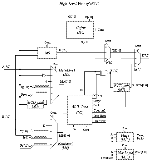
High-Level Model of c3540
Statistics: 50 inputs; 22 outputs; 1669 gates
Function: 8-bit ALU with binary and BCD arithmetic, and logic and shift operations.
This benchmark is an 8-bit ALU that can perform binary and BCD arithmetic operations as well as logic and shift operations. Logic operations are intermixed with arithmetic ones, much as in the TTL 74181. BCD addition is done via a two's-complement adder by adding 6 to both digits of the first operand, and then subtracting 6 from the digits of the result if they do not generate a carry. A total of 14 control inputs are used for multiplexing and masking data inputs. Most multiplexers in this circuit have an odd-number of inputs, e.g, 3 and 5, and their selection is different between lower and upper digits (4 bits). The selection mechanism of M4 (output MB) is even more complicated; see below for details. The largest module is M5 (ALU_Core), which consists of two 4-bit CLAs. Module M8 (Shifter) can shift the input bus A by 1 to 8 bits in either direction. Parity and zero flags are generated by module M12 (Flags) using the input buses A, B and the output bus Z; see the relevant figures or the Verilog model for their exact definition. Various logic functions of A and B are calculated by module M13 which does not have an apparent high-level structure.
Inputs/Outputs vs. Netlist Numbers
Models:
- I. Original ISCAS gate-level netlist
- II. Verilog hierarchical netlist (functionally equivalent to I)
- III. Verilog flat netlist (flat version of II; functionally equivalent to I, but with minor structural differences)
Modules M1 (BCD_add) and M7 (BCD_sub)
In order to perform BCD addition with a two's complement adder, module M1 adds 6 to each digit of the input bus, and module M7 subtracts 6 from each digit of the result if there is no carry from that digit.
The logic equations for the lower digit of M1 (upper digit is similar):
The logic equations for the lower digit of M7 (upper digit is similar):
- Out[3] = In[3].Carry4 + In[3]. In[2] . In[1]. !Carry4
- Out[2] = In[2] In[1]. !Carry4
- Out[1] = In[1] !Carry4
- Out[0] = In[0]
Module M3 (MainMux1)
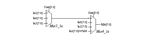
This module consists of two cascaded multiplexers, as shown above. The control signals Cont[3:0] determine the select inputs of M3. Notice that selection is different between the lower and the upper digits of the output.
Module M4 (MainMux2)
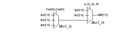
Like M3, Module M4 is made up of two cascaded multiplexers. However, it's select logic is more involved. The control signals Cont[6:3] and Cont[1:0] are decoded into the following select signals:
- CHi = Cont[0]. Cont[1]. !(Cont[3]. Cont[5])
- CLo1 = !Cont[0]. !Cont[5]. Cont[6]
- CLo2 = !Cont[0]. Cont[6]
- CLo3 = !Cont[0]. (Cont[5]+Cont[6])
Notice that since In1 is connected to the single bit K input, all the bits of MB can be set to K (0 or 1).
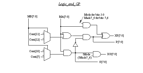
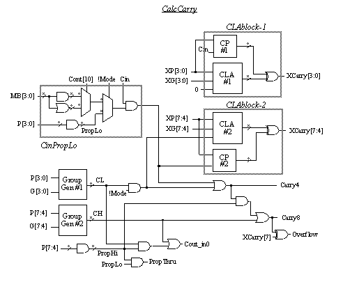
Module M5 (ALU_Core)
This is the largest module of the c3540 benchmark. The control inputs to this module are Cont[12:7] and Cont[2:0]. An internal signal called Mode determines whether a logic or an arithmetic operation is to be performed:
Mode is 1 for a logic operation, and 0 for an arithmetic operation. In the case of arithmetic operations, an additional control signal named Mask7_6 is used to mask bits #7 and #6 of the MA bus:
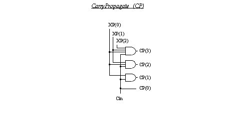
As in the TTL circuit 74181, logic and arithmetic operations are intermixed. A block named Logic_and_GP computes both logic operations as well as the generate and propagate signals used for binary addition. The carry signals are computed by CalcCarry, and the final result of the ALU is obtained by XORing the carry signals with a modified propagate signal called XP.
The set of logic and arithmetic operations performed by ALU_Core is shown below. The table is valid for Cin=0. Logic 1 is added to the result if Cin=1 (this applies to arithmetic as well as logic operations.)
Legend for operators:
- ! : complement
- + : logical OR
- . : logical AND
- xor : logical XOR
- xnor : logical XNOR
- plus : arithmetic add
- minus: arithmetic subtract
Module M8 (Shifter)
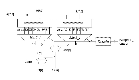
This module contains logic for shifting the input bus A by 1 to 8 bits in either direction. When shifting towards LSB (MSB), the empty bit positions are filled by a Q (R) bus. The Shifter decodes the control signals Cont[12:10], and Cont[2] into 8 signals, which are the select inputs for sixteen 8:1 multiplexers. Input selection for these multiplexers is shown below. The X and Y buses are fed into a 2:1 multiplexer controlled by Cont[3]. There is an additional multiplexer for bit #7 whose second input is A[7]; this can be used for shifting signed input data.
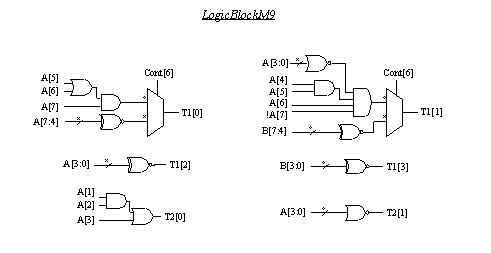
Module M9
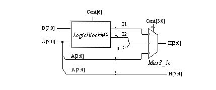
This is a relatively small module that appears to calculate some special-purpose logic functions of the input buses A and B. Five control inputs to this module are Cont[6] and Cont[3:0]. The select inputs of the 3:1 multiplexer Mux3_1c are calculated by
The details of LogicBlockM9 are shown below. It seems to calculate a non-standard function. It may be some type of code translation or encryption. The authors will be glad to know if you have any insight into the function of this particular block. Please contact us if you have any information.
Module M10
This module contains a set of eight 3:1 multiplexers of type Mux3_1c. As with the other multiplexers, the lower and upper digits of the output are selected differently. The control signals Cont[7],Cont[3:0] are decoded into three select signals CHi, CLo1, CLo2 as follows.
- CHi = !(Cont[0]. Cont[1]. (!Cont[2] + Cont[7]))
- CLo1 = Cont[1]+Cont[2]+Cont[3]
- CLo2 = Cont[1]+Cont[3]
Module M11
This module consists of eight 3:1 multiplexers of type Mux3_1c. Unlike M10, its lower and upper digits are selected by the same two signals which are decoded from the control signals Cont[6:5], Cont[2:0] as follows.
Module M12 (Flags)
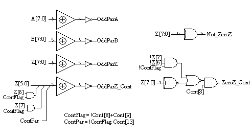
This module generates two zero flags and four parity outputs. As shown above, the parities are calculated from the input buses A and B, and the output bus Z. The zero flags are calculated from the output bus Z only. Three control inputs to M12 are Cont[13] and Cont[9:8]. Paralleling the type of masking used in ALU_Core by Mask7_6, this module can mask out Z[7:6] for the OddParZ_Cont and ZeroZ_Cont outputs using an internally generated ContFlag signal.
|
Input |
|
|---|---|
|
2897, 200, 190, 179, 343, 213, 169, 45, 41, 1698, 33, 20, 13, 1 |